First, the structure and properties of SiC crystal.
SiC is a binary compound formed by Si element and C element in 1:1 ratio, that is, 50% silicon (Si) and 50% carbon (C), and its basic structural unit is SI-C tetrahedron.

Schematic diagram of silicon carbide tetrahedron structure
For example, Si atoms are large in diameter, equivalent to an apple, and C atoms are small in diameter, equivalent to an orange, and an equal number of oranges and apples are piled together to form a SiC crystal.
SiC is A binary compound, in which the Si-Si bond atom spacing is 3.89 A, how to understand this spacing? At present, the most excellent lithography machine on the market has a lithography accuracy of 3nm, which is a distance of 30A, and the lithography accuracy is 8 times that of the atomic distance.
The Si-Si bond energy is 310 kJ/mol, so you can understand that the bond energy is the force that pulls these two atoms apart, and the greater the bond energy, the greater the force that you need to pull apart.

We know that every substance is made up of atoms, and the structure of a crystal is a regular arrangement of atoms, which is called a long-range order, like the following. The smallest crystal unit is called a cell, if the cell is a cubic structure, it is called a close-packed cubic, and the cell is a hexagonal structure, it is called a close-packed hexagonal.

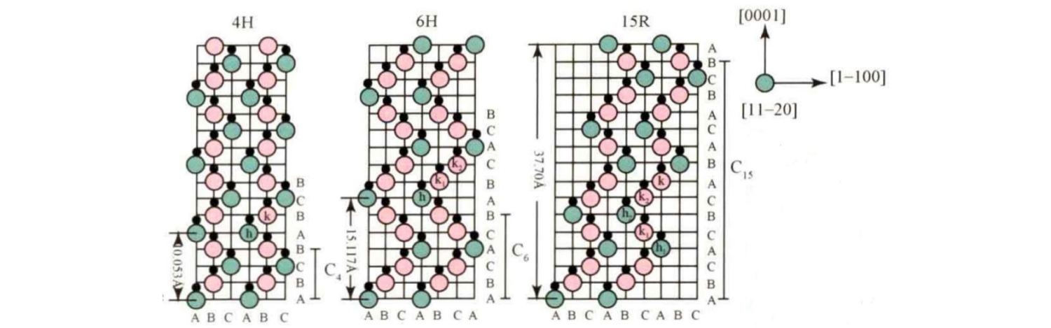
Common SiC crystal types include 3C-SiC, 4H-SiC, 6H-SiC, 15R-SiC, etc. Their stacking sequence in the c axis direction is shown in the figure.

Among them, the basic stacking sequence of 4H-SiC is ABCB... ; The basic stacking sequence of 6H-SiC is ABCACB... ; The basic stacking sequence of 15R-SiC is ABCACBCABACABCB... .
This can be seen as a brick for building a house, some of the house bricks have three ways of placing them, some have four ways of placing them, some have six ways.
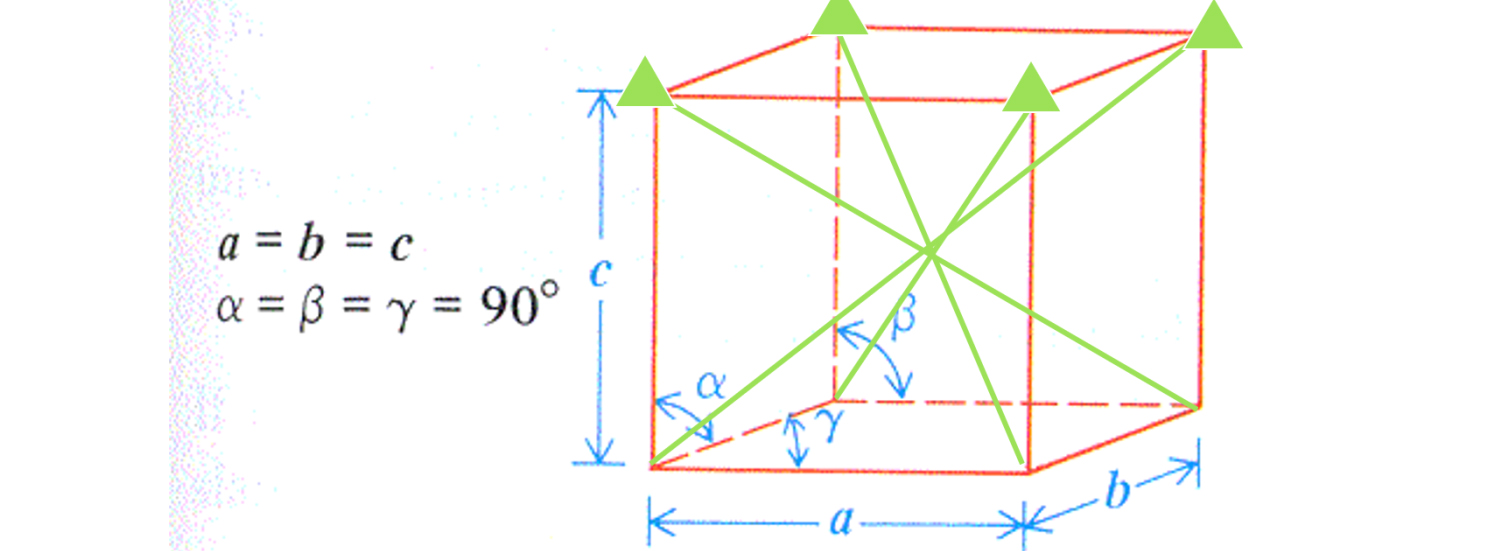
The basic cell parameters of these common SiC crystal types are shown in the table:

What do a, b, c and angles mean? The structure of the smallest unit cell in a SiC semiconductor is described as follows:
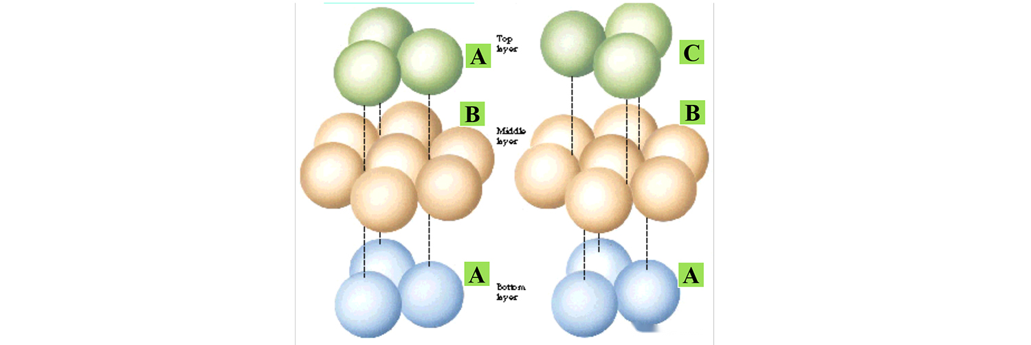
In the case of the same cell, the crystal structure will also be different, this is like we buy the lottery, the winning number is 1, 2, 3, you bought 1, 2, 3 three numbers, but if the number is sorted differently, the winning amount is different, so the number and the order of the same crystal, can be called the same crystal.
The following figure shows the two typical stacking modes, only the difference in the stacking mode of the upper atoms, the crystal structure is different.
The crystal structure formed by SiC is strongly related to temperature. Under the action of high temperature of 1900~2000 ℃, 3C-SiC will slowly transform into hexagonal SiC polyform such as 6H-SiC because of its poor structural stability. It is precisely because of the strong correlation between the probability of formation of SiC polymorphs and temperature, and the instability of 3C-SiC itself, the growth rate of 3C-SiC is difficult to improve, and the preparation is difficult. The hexagonal system of 4H-SiC and 6H-SiC are the most common and easier to prepare, and are widely studied due to their own characteristics.
The bond length of SI-C bond in SiC crystal is only 1.89A, but the binding energy is as high as 4.53eV. Therefore, the energy level gap between the bonding state and the anti-bonding state is very large, and a wide band gap can be formed, which is several times that of Si and GaAs. The higher band gap width means that the high-temperature crystal structure is stable. The associated power electronics can realize the characteristics of stable operation at high temperatures and simplified heat dissipation structure.
The tight binding of the Si-C bond makes the lattice have a high vibration frequency, that is, a high energy phonon, which means that the SiC crystal has a high saturated electron mobility and thermal conductivity, and the related power electronic devices have a higher switching speed and reliability, which reduces the risk of device overtemperature failure. In addition, the higher breakdown field strength of SiC allows it to achieve higher doping concentrations and have lower on-resistance.
Second, the history of SiC crystal development
In 1905, Dr. Henri Moissan discovered a natural SiC crystal in the crater, which he found resembled a diamond and named it the Mosan diamond.
In fact, as early as 1885, Acheson obtained SiC by mixing coke with silica and heating it in an electric furnace. At the time, people mistook it for a mixture of diamonds and called it emery.
In 1892, Acheson improved the synthesis process, he mixed quartz sand, coke, a small amount of wood chips and NaCl, and heated it in an electric arc furnace to 2700℃, and successfully obtained scaly SiC crystals. This method of synthesizing SiC crystals is known as the Acheson method and is still the mainstream method of producing SiC abrasives in industry. Due to the low purity of synthetic raw materials and rough synthesis process, Acheson method produces more SiC impurities, poor crystal integrity and small crystal diameter, which is difficult to meet the requirements of the semiconductor industry for large-size, high-purity and high-quality crystals, and cannot be used to manufacture electronic devices.
Lely of Philips Laboratory proposed a new method for growing SiC single crystals in 1955. In this method, graphite crucible is used as the growth vessel, SiC powder crystal is used as the raw material for growing SiC crystal, and porous graphite is used to isolate a hollow area from the center of the growing raw material. When growing, the graphite crucible is heated to 2500℃ under the atmosphere of Ar or H2, and the peripheral SiC powder is sublimed and decomposed into Si and C vapor phase substances, and the SiC crystal is grown in the middle hollow region after the gas flow is transmitted through the porous graphite.

Third, SiC crystal growth technology
The single crystal growth of SiC is difficult due to its own characteristics. This is mainly due to the fact that there is no liquid phase with a stoichiometric ratio of Si: C = 1:1 at atmospheric pressure, and it cannot be grown by the more mature growth methods used by the current mainstream growth process of the semiconductor industry - cZ method, falling crucible method and other methods. According to theoretical calculation, only when the pressure is greater than 10E5atm and the temperature is higher than 3200℃, the stoichiometric ratio of Si: C = 1:1 solution can be obtained. In order to overcome this problem, scientists have made unremitting efforts to propose various methods to obtain high crystal quality, large size and cheap SiC crystals. At present, the main methods are PVT method, liquid phase method and high temperature vapor chemical deposition method.
Post time: Jan-24-2024