
SiC Etching Process Parts
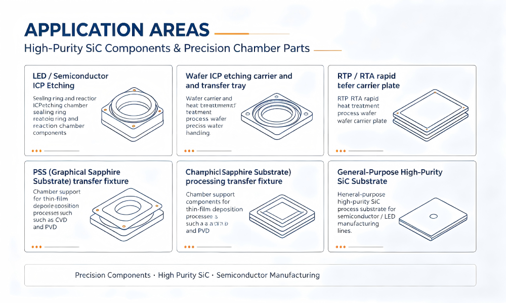
Etching process parts are critical functional components within process chambers for ICP etching, CVD, and rapid thermal treatment (RTP/RTA) in semiconductor and LED manufacturing. They are subject to stringent requirements regarding material purity, plasma corrosion resistance, surface flatness, and particle contamination control. Semicera utilizes high-purity silicon carbide (SiC) substrates and further enhances surface density and corrosion resistance through a CVD SiC coating process. The resulting products achieve a purity exceeding 99.99995% and a surface roughness as low as Ra<0.1μm. These parts are widely applied in LED/semiconductor ICP etching chamber sealing rings, wafer carriers/transit trays, and RTP/RTA rapid thermal treatment support plates, serving as essential consumables that ensure yield rates and equipment stability in etching and thermal treatment processes.
Product Technical Specifications
|
Product name |
Material/Crafting |
Fineness |
Surface roughness |
Typical Applications |
|
CVD SiC coating / high-purity SiC substrate |
≥99.9995% |
Ra<0.2μm |
LED/semiconductor ICP and CVD etching chamber sealing rings, resistant to plasma bombardment and chemical corrosion, reducing process particle contamination |
|
|
Reaction-sintered SiC + CVD SiC coating |
≥99.999% |
Ra<0.1μm |
Carrying and transporting wafers in LED/semiconductor ICP etching processes: multi-position/multi-wafer design enhances production capacity |
|
|
Reactively sintered silicon carbide (RBSiC) |
≥99.99% |
Ra<0.3μm |
General-purpose process chamber carrier substrate, featuring high temperature and corrosion resistance; customizable for various hole layouts and substrate specifications. |
|
|
CVD SiC coating / high-purity SiC substrate |
≥99.9995% |
Ra<0.1μm |
Wafers are supported for RTP/RTA rapid heat treatment and PSS patterned substrate processes, ensuring uniform heat transfer and rapid temperature response. |
Core Performance Advantages
- Ultra-high purity: The SiC substrate can achieve a purity exceeding 99.999%, effectively reducing contamination by metal ions and particles during the manufacturing process.
- Plasma corrosion resistance: The CVD SiC coating is dense and uniform, significantly enhancing the corrosion resistance lifespan of components in ICP and CVD etching chambers.
- High surface flatness: surface roughness as low as Ra<0.1μm, reducing back-side damage to wafers and the residual presence of process particles.
- Excellent thermal conductivity uniformity: enables rapid and uniform temperature rise and fall during RTP/RTA rapid heat treatment, thereby enhancing temperature uniformity.
- High mechanical strength and wear resistance: Resists deformation and wear even under prolonged operation in vacuum/plasma environments, thereby reducing replacement frequency.
- High degree of customization: hole positions, thickness, number of support plates, and overall dimensions can be tailored to match the customer's equipment model.
Application area
Why choose Semicera?
- • End-to-end quality control: key parameters—including purity, surface roughness, and resistivity—can be supported by third-party test reports.
- • Support for non-standard customized manufacturing: hole positions, dimensions, thickness, and bearing plate specifications can all be customized according to the customer's equipment drawings.
- • Stable supply capacity: Standardized production processes ensure batch consistency, supporting both regular and urgent deliveries.
- • Technical Support: Our engineering team can provide equipment selection recommendations tailored to specific machine models and process requirements.
FAQ
Q: Why is silicon carbide (SiC) commonly selected for components in etching processes?
A: Silicon carbide exhibits excellent plasma corrosion resistance, high purity, high thermal conductivity, and superior mechanical strength. Under high-energy plasma conditions in etching chambers—such as those used in ICP/CVD—it is resistant to erosion, minimizes impurity release, effectively reduces wafer contamination risks, and extends component service life. Consequently, silicon carbide has become a mainstream material choice in semiconductor and LED manufacturing processes.
Q: What are the differences between CVD SiC coatings and reaction-sintered SiC substrates?
A: Reactively sintered SiC (RBSiC) is a substrate body forming process that offers excellent structural strength and cost advantages; CVD SiC coating involves the formation of a dense, high-purity silicon carbide coating on the substrate surface via chemical vapor deposition, which further enhances surface purity, corrosion resistance, and gas tightness. This technique is commonly employed for surface treatment of components—such as etching rings and wafer carriers—that require extremely stringent contamination control.
Q: How does the surface roughness of the SiC wafer carrier disk affect the manufacturing process?
A: Surface roughness directly affects the back-side contact condition of the wafer and the uniformity of heat transfer. Excessive roughness can lead to back-side damage of the wafer, particle residue, or temperature unevenness, which in turn compromises etching uniformity and yield; therefore, components in direct contact with the wafer—such as support plates and substrate plates—typically require a high surface flatness with an Ra value of <0.1–0.3 μm.
Q: Can the SiC substrate discs used for RTP/RTA be interchangeably used with those used for ICP etching trays?
A: Although both types share similar substrates, their process design priorities differ: RTP/RTA substrates prioritize thermal conductivity uniformity and rapid temperature rise/cooling response to ensure uniform wafer temperature distribution; ICP etching trays, on the other hand, emphasize plasma corrosion resistance and surface contamination control. It is recommended to select the appropriate type based on the specific process chamber and machine model; if cross-process usage is required, please confirm compatibility with your technical engineers.
Contact us
If you require detailed technical datasheets, test reports, or customized solutions for your etching process components, please feel free to request a quote or contact our team of technical engineers.


