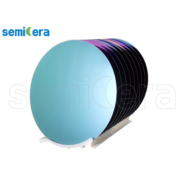
Product Overview
Silicon On Insulator (SOI) wafers use a three-layer structure: a thin silicon device layer, a buried oxide (BOX) insulating layer, and a silicon handle substrate. The silicon dioxide layer electrically isolates active devices from the substrate, significantly reducing parasitic capacitance and leakage current. The result is higher switching speed, lower power consumption, and improved immunity to noise and high temperatures.
Semicera offers SOI wafers in a wide range of specifications. Device layer thickness, BOX thickness, crystal orientation, doping type and resistivity can all be tailored to your requirements, supporting everything from R&D prototyping to volume production.
Key Features
- • Excellent electrical isolation: The buried oxide suppresses substrate coupling and reduces parasitic capacitance and leakage.
- • Low power, high speed: Lower power consumption and faster switching compared with bulk silicon.
- • Latch-up and radiation resistance: Well suited to high-reliability and harsh-environment applications.
- • High-temperature performance: Lower leakage and stable operation at elevated temperatures.
- • High uniformity: Tight thickness uniformity for device and BOX layers, low surface roughness, and low particle counts.
- • Flexible customization: Thickness, orientation, doping and resistivity tailored to your design.
Specifications
|
Parameter |
Specification |
|
Wafer Diameter |
100 mm / 150 mm / 200 mm / 300 mm |
|
Manufacturing Process |
Smart Cut™ / Bonded & Etch-back (BESOI) / SIMOX |
|
Device Layer Thickness |
50 nm – 100 μm (customizable) |
|
Buried Oxide (BOX) Thickness |
100 nm – 3 μm (customizable) |
|
Device Layer Orientation |
⟨100⟩ / ⟨111⟩ / ⟨110⟩ |
|
Conductivity Type |
P-type / N-type |
|
Resistivity |
Customizable, including high-resistivity (HR-SOI) |
|
Handle Wafer Thickness |
Depends on diameter (e.g., 725 μm for 200 mm) |
|
Surface Roughness |
≤ 0.5 nm (AFM, 5 × 5 μm) |
|
Particles |
Per specification; customer requirements supported |
|
Packaging |
Cleanroom packaging, 25 wafers per cassette |
Applications

Why Choose Semicera
- • Consistent quality: Strict incoming inspection and outgoing testing ensure lot-to-lot consistency.
- • Customization capability: From small sample runs to volume supply.
- • Responsive support: Our technical team assists with selection and process questions.
- • Clean packaging and logistics: End-to-end contamination control for safe delivery.
Frequently Asked Questions
Q1: How does an SOI wafer differ from a standard silicon wafer?
An SOI wafer includes a buried oxide layer that isolates devices from the substrate, enabling higher speed, lower power consumption and better noise immunity.
Q2: Which sizes and thicknesses can be customized?
We support 4, 6, 8 and 12 inch wafers. Device layer and BOX thickness can be customized; please contact us to confirm specific requirements.
Q3: Can I request samples?
Yes. Please send us the diameter, device layer/BOX thickness, orientation and doping requirements, and we will respond promptly.
Q4: What is the minimum order quantity?
We support both small sample orders and volume orders. Please contact our sales team for details.