Application field
1. High-speed integrated circuit
2. Microwave devices
3. High temperature integrated circuit
4. Power devices
5. Low power integrated circuit
6. MEMS
7. Low voltage integrated circuit
|
Item |
Argument |
|
|
Overall |
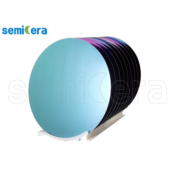
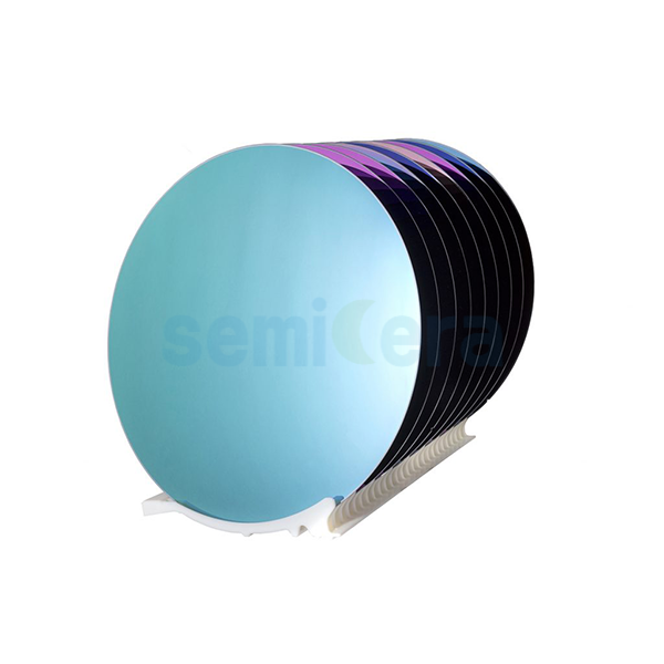
Wafer Diameter |
50/75/100/125/150/200mm±25um |
|
Bow/Warp |
<10um |
|
|
Particles |
0.3um<30ea |
|
|
Flats/Notch |
Flat or Notch |
|
|
Edge Exclusion |
/ |
|
|
Device Layer |
Device-layer Type/Dopant |
N-Type/P-Type |
|
Device-layer Orientation |
<1-0-0> / <1-1-1> / <1-1-0> |
|
|
Device-layer Thickness |
0.1~300um |
|
|
Device-layer Resistivity |
0.001~100,000 ohm-cm |
|
|
Device-layer Particles |
<30ea@0.3 |
|
|
Device Layer TTV |
<10um |
|
|
Device Layer Finish |
Polished |
|
|
BOX |
Buried Thermal Oxide Thickness |
50nm(500Å)~15um |
|
Handle Layer |
Handle Wafer Type/Dopant |
N-Type/P-Type |
|
Handle Wafer Orientation |
<1-0-0> / <1-1-1> / <1-1-0> |
|
|
Handle Wafer Resistivity |
0.001~100,000 ohm-cm |
|
|
Handle Wafer Thickness |
>100um |
|
|
Handle Wafer Finish |
Polished |
|
|
SOI wafers of target specifications can be customized according to customer requirements. |
||