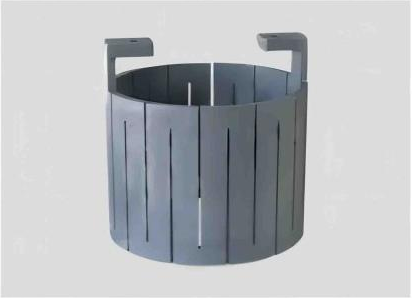
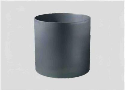
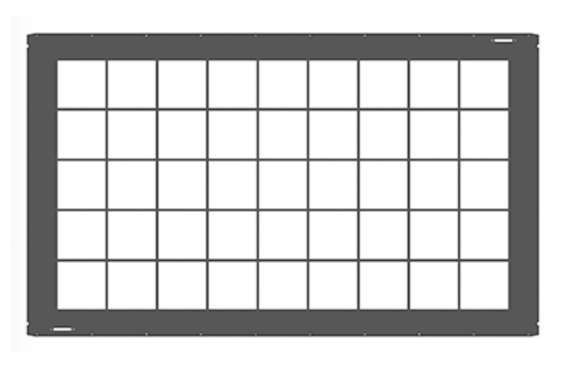
SiC Wafer Boat
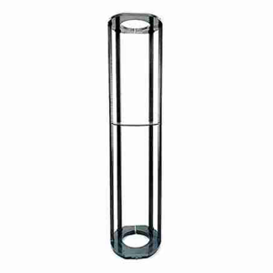
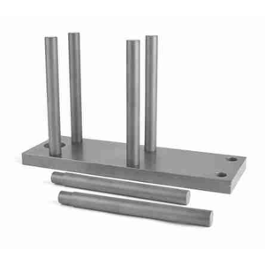
Silicon carbide wafer boat is a load-bearing device for wafers, mainly used in solar and semiconductor diffusion processes. It has characteristics such as wear resistance, corrosion resistance, high-temperature impact resistance, resistance to plasma bombardment, high temperature bearing capacity, high thermal conductivity, high heat dissipation, and long-term use that is not easy to bend and deform. Our company uses high-purity silicon carbide material to ensure service life and provides customized designs, including. various vertical and horizontal wafer boat.
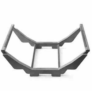
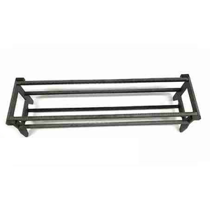
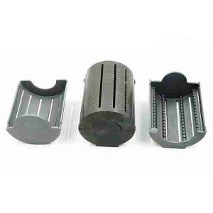
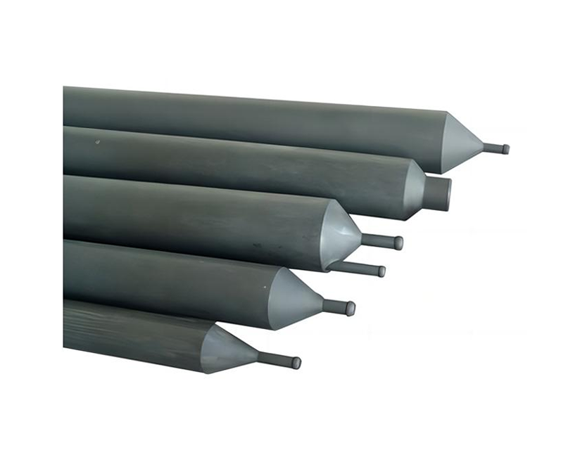
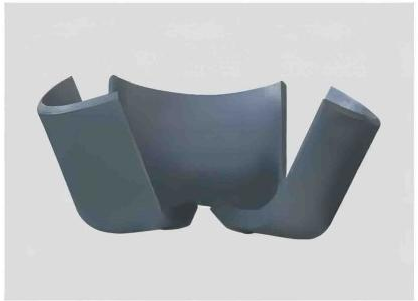
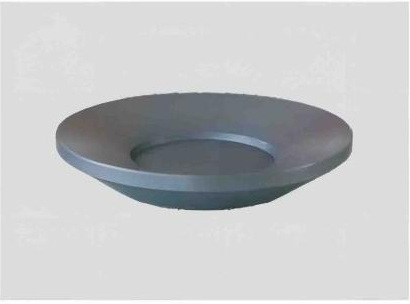
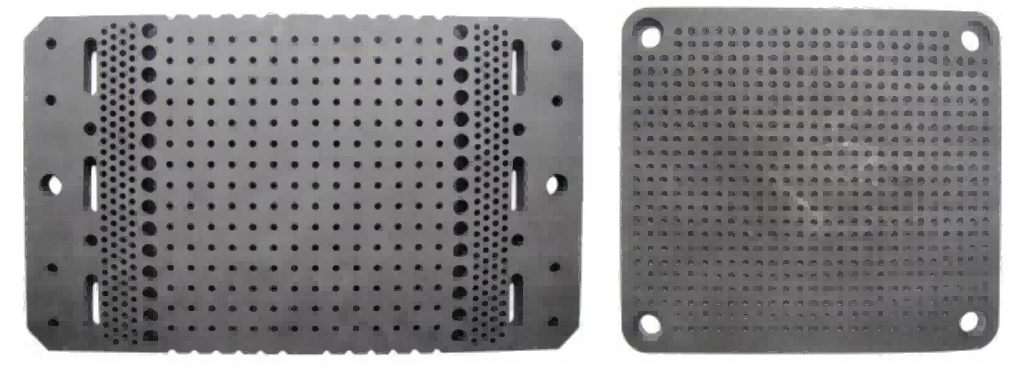
SiC Paddle
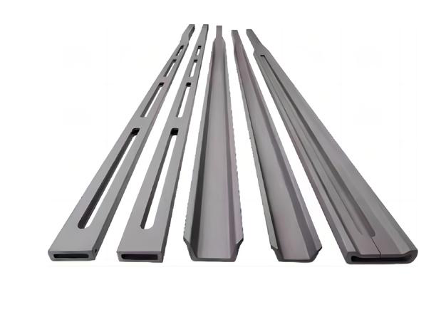
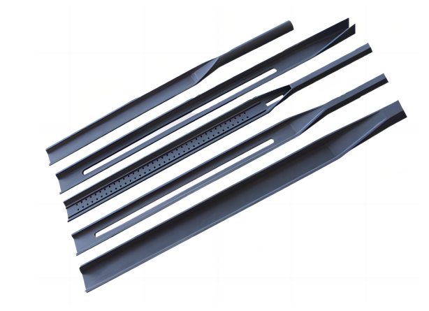
The silicon carbide cantilever paddle is mainly used in the (diffusion) coating of silicon wafers, which plays a crucial role in the loading and transportation of silicon wafers at high temperature. It is a key component of semiconductor wafer loading systems and has the following main characteristics:
1. It does not deform in high temperature environments and has a high loading force on the wafers;
2. It is resistant to extreme cold and rapid heat, and has a long service life;
3. The thermal expansion coefficient is small, greatly extending the maintenance and cleaning cycle, and significantly reduce pollutants.
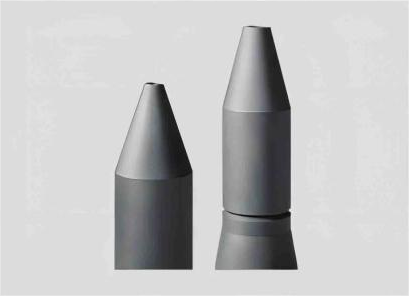
SiC Furnace Tube
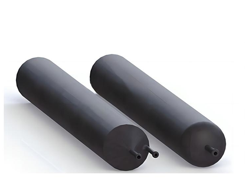
Silicon carbide process tube, made of high-purity SiC without metallic impurities, does not pollute the wafer, and is suitable for processes such as semiconductor and photovoltaic diffusion, annealing and oxidation process.
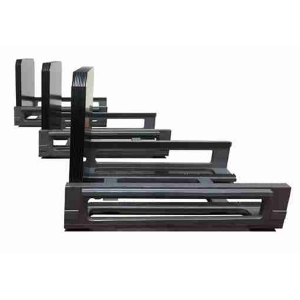
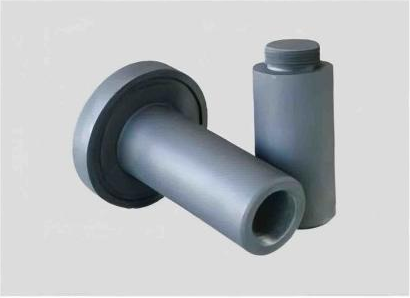
SiC Robot Arm
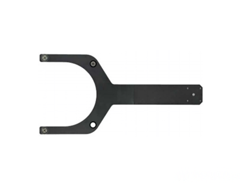
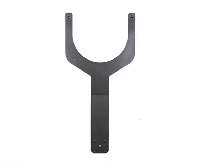
SiC robot arm, also known as wafer transfer end effector, is a robotic arm used to transport semiconductor wafers and is widely used in the semiconductor, optoelectronic, and solar energy industries. Using high-purity silicon carbide, with high hardness, wear resistance, seismic resistance, long-term use without deformation, long service life,etc, can provide customized services.
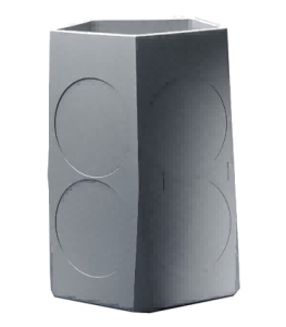
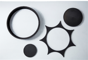
Graphite for crystal growth
Graphite heat shield
Graphite electrode tube
Graphite deflector
Graphite chuck
All processes used for growing semiconductor crvstals operate in high-temperature and corrosive environments. The hot zone of the crystal growth furnace is usually eguinned with heat-resistant and corrosion-resistant high purity. graphite components, such as graphite heaters, crucibles, cylinders, deflector, chucks, tubes,rings, holders,nuts,etcl Our finished product can achieve an ash content less than 5ppm.
Graphite for Semidonductor Epitaxy
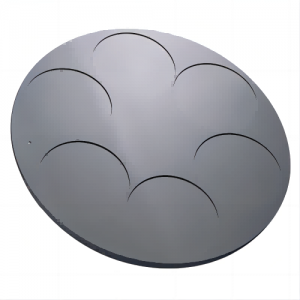
Graphite Base
Graphite Epitaxial Barrel
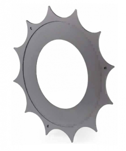
Monocry Stalline Silicon Epitaxial Base
MOCVD Graphite Parts
Semiconductor Graphite Fixture
Epitaxial process refers to the growth of a single crystal material on a single crystal substrate with the same lattice arrangement as the substrate. It requires many ultra-high purity graphite parts and graphite base with SIC coating. The high purity graphite used for semiconductor epitaxy has a wide range of applications, which can match most commonly used equipment in the industry, At the same time, it has extremely high. purity, uniform coating, excellent service life, and extremely high chemical resistance and thermal stability.
Insulation Material and other
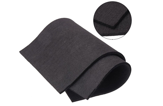
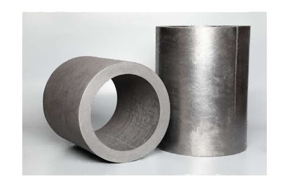
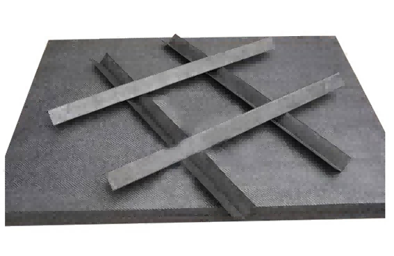
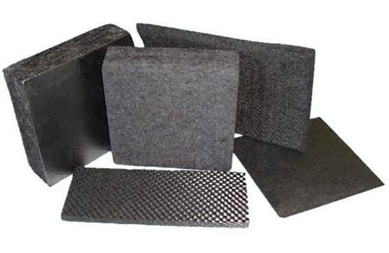
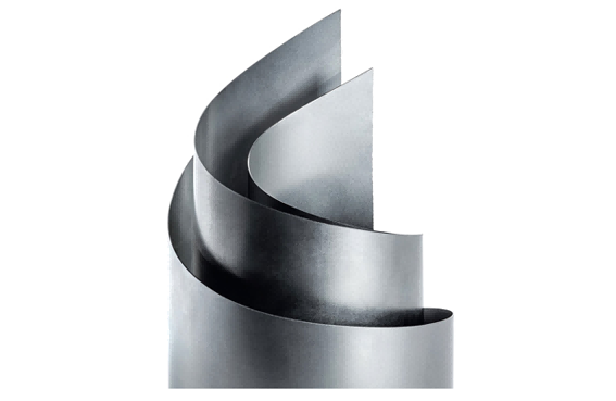
Thermal insulation materials used in semiconductor production are graphite hard felt, soft felt, graphite foil, carbon composite materials, etc. Our raw materials are imported graphite materials, which can be cut according to the specification of customers, and can also be sold as a whole. Carbon composite material is usually used as a carrier for solar monocrystal and polysilicon cell production process.