Purification and Mappings
Our service covers the purification and mapping of a wide range of semiconductor materials, with the aim of delivering high-quality semiconductor materials for various applications. Leveraging our advanced purification technology and state-of-the-art equipment, we effectively eliminate impurities, thereby enhancing the purity of semiconductor materials. Our purification process is meticulously designed, incorporating multiple steps and strict quality control measures to ensure exceptional purity and stability of the materials we offer.
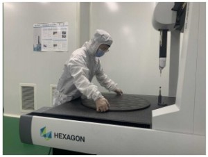
Additionally, we are dedicated to providing our customers with precise and reliable mapping services. Equipped with advanced testing equipment and instruments, and supported by a team of experienced professionals, we are capable of conducting comprehensive measurements and analyses of semiconductor material characteristics. Our mapping services encompass a wide range of tests, including electrical properties, composition, purity, physical properties, and thorough investigations into material structure and composition. Through meticulous mapping, we gather detailed data and information, enabling us to provide customers with accurate assessments of material characteristics and relevant recommendations.
Machinery Capability
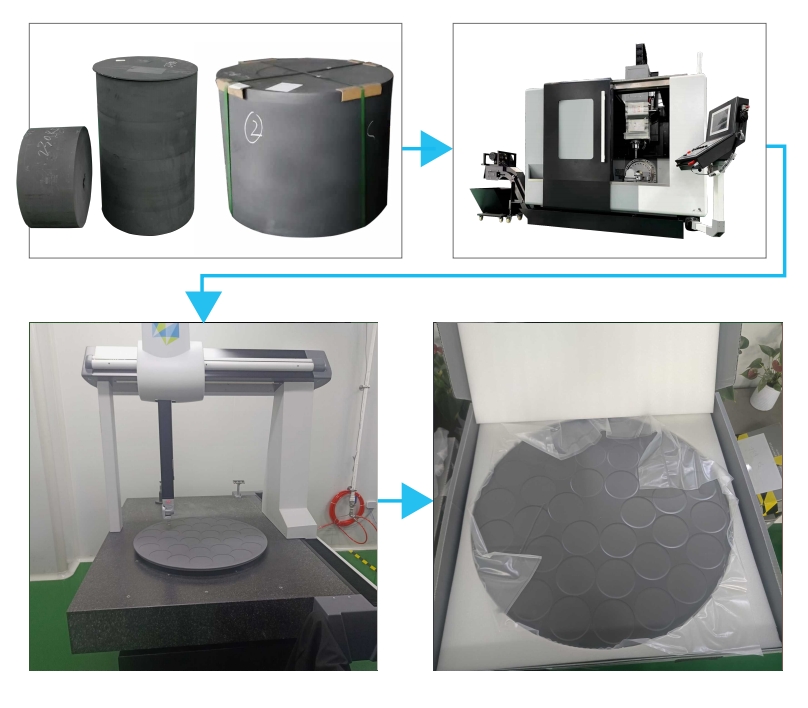
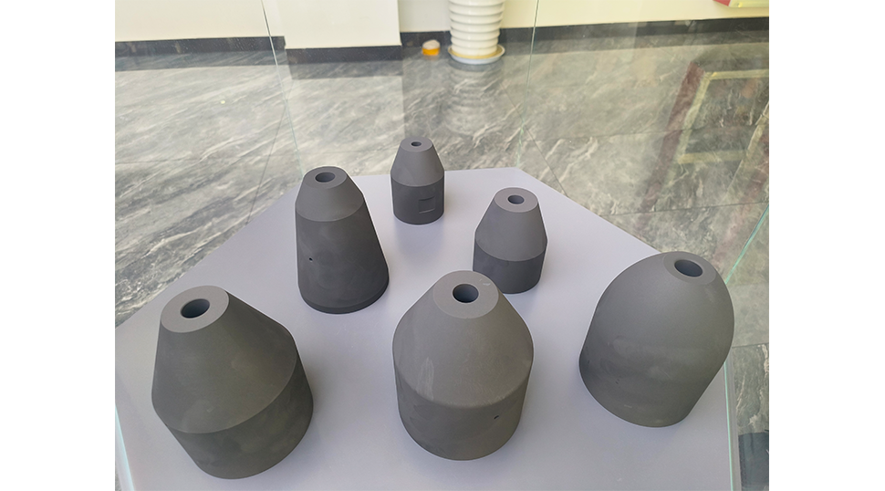
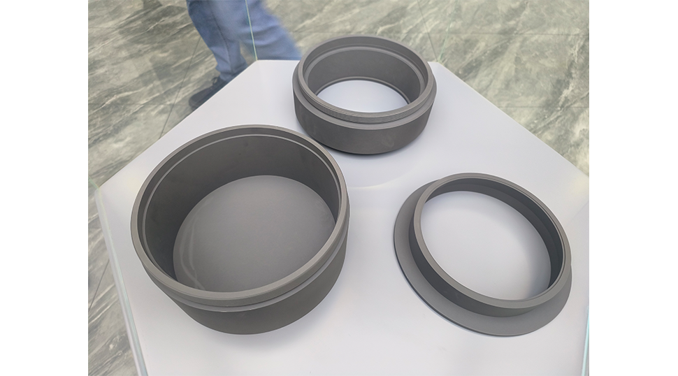
Semicera Semiconductor has a leading semiconductor field of graphite, silicon carbide and other machining capabilities and experience, can meet customers for semiconductor products of high precision, high purity, high quality and other processing needs. The tools we use, the cutting process and the choice of materials are also carefully optimized to achieve micron size control and high surface quality. We pay attention to quality control and process optimization in the processing process, realtime monitoring and control of key parameters in the processing process to ensure product consistency and stability. We also implement a strict quality management system to ensure that products are processed in accordance with customerl requirements and industry standards, and carry out comprehensive quality inspection.
We will continuously invest in equipment improvement and technological innovation to meet the growing needs of our customers and provide them with superior solutions and support.
Solution of Thermal Field Modification
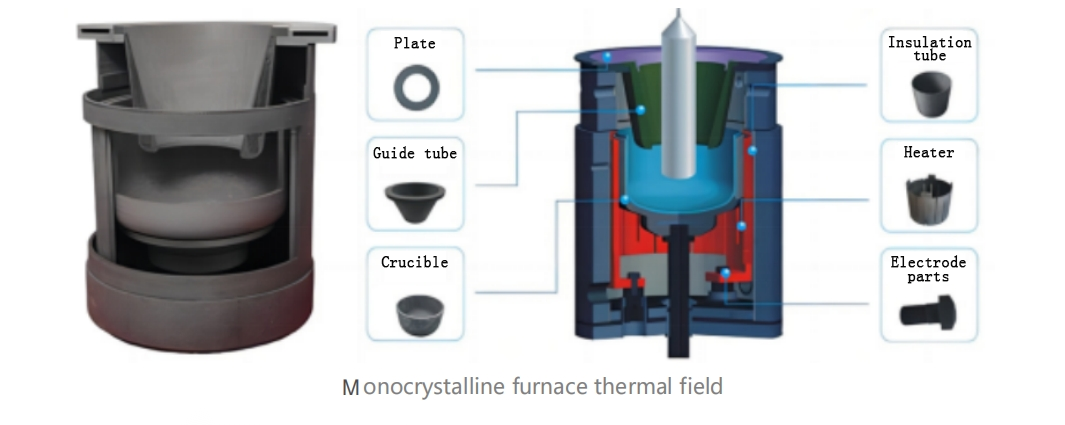
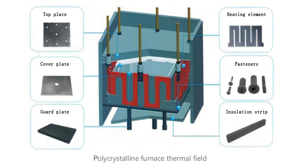
In terms of thermal field design and transformation, our company can complete the design and batch supply to Czochra single crystal, casting polycrystal, gallium arsenide, zinc selenide, sapphire, silicon carbide and other different industry equipment. At the same time, for the mechanical thermal calculation of various structures, components and atmospheres under different high temperature environments, we also have professional modeling and simulation computing capabilities, which can provide customers with professional design optimization programs and suggestions.

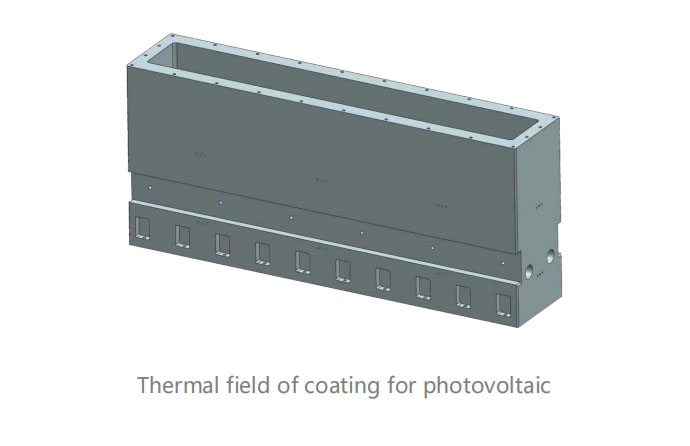
In the process of manufacturing solar cells, the preparation of anti reflective films is an essential process. Main anti reflective films include silicon nitride/silicon oxide, which not only have the function of anti reflective films but also have passivation effects. The preparation of anti reflective films mainly relies on plasma enhanced vapor deposition (PECVD) method.
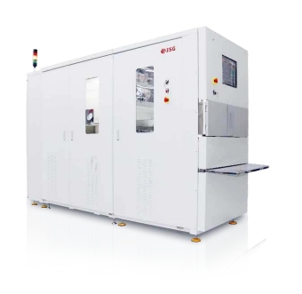
We provide efficient solutions by using the latest designed PECVD silicon wafer carriers made of isostatic graphite or carbon fiber reinforced materials, such as graphite boats and graphite frames, and provide the purification and coating services, to enhance material performance.
Semiconductor Product Test Kits
We are committed to providing various semiconductor thermal field product test kits to meet the different needs ofl customers. Our testings cover a wide range of semiconductor materials, including silicon carbide, graphite, tantaluml carbide, etc., for comprehensive testing of the electrical properties, composition, purity, physical properties, size, andl crystal structure. These testing kits are designed and manufactured by a professional team, equipped with advancedl testing equipments and instruments to ensure high accuracy and reliability. Our product testing kits not only provides a comprehensive testing plan, but also includes detailed testing reports and analysis to help customers understandl the performance and potential issues of the product.
GDMS
D-SIMS