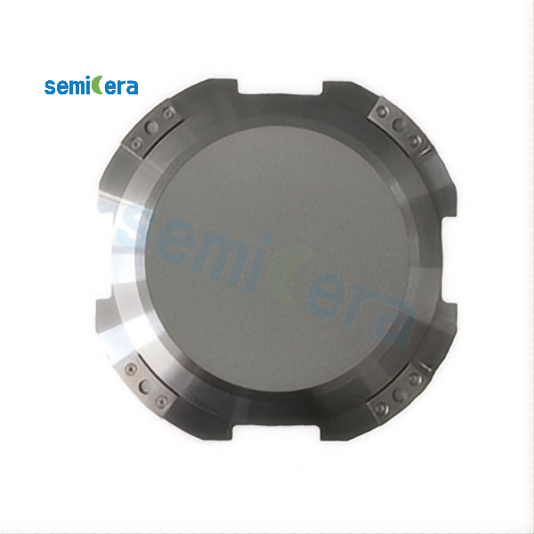
Aluminum Nitride (AlN) Wafer
Semicera's aluminum nitride (AlN) wafers are grown using the Physical Vapor Transport (PVT) method in-house; these wafers feature an ultra-wide bandgap (~6.2 eV), exceptional thermal conductivity, outstanding electrical insulation properties, and superior lattice quality, making them the core substrate material for next-generation high-power RF devices, high-voltage power electronic devices, and deep-ultraviolet optoelectronic devices. As a leading Chinese enterprise specializing in the research, development, production, and sales of ultra-wide bandgap AlN monocrystalline substrates, headquartered in Ningbo, Zhejiang Province, Semicera focuses on achieving breakthroughs in AlN monocrystalline core technologies, providing critical core material support for China's fourth-generation semiconductor high-end devices, the energy revolution, and national defense security.
Core Performance Advantages
|
Material characteristics |
Si |
GaAs |
InP |
SiC |
GaN |
Diamond |
Ga₂O₃ |
AlN |
|
Band gap(eV) |
1.12 |
1.4 |
1.3 |
3.2 |
3.4 |
5.5 |
4.8 |
6.2 |
|
Dielectric constant |
11.7 |
13.1 |
12.5 |
9.7 |
9.8 |
5.7 |
10 |
8.7 |
|
Breakdown electric field strength (MV/cm) |
0.3 |
0.4 |
0.5 |
2.2 |
3.3 |
6 |
8 |
12 |
|
Saturation velocity (10⁷ cm/s) |
1 |
2 |
1 |
2 |
2.5 |
2.7 |
2 |
2 |
|
Thermal conductivity (W/cm·K) |
1.5 |
0.5 |
0.7 |
4.5 |
2-3 |
22 |
0.1-0.3 |
3.2 |
|
Electron mobility (cm²/V·s) |
1350 |
8500 |
5400 |
900 |
1000 |
2000 |
300 |
500 |
The outstanding advantages of AlN: it boasts the highest bandgap and highest breakdown electric field strength among all material systems, along with exceptional thermal conductivity (~320 W/m·K – significantly exceeding that of high-quality ceramics (<250 W/m·K)), extremely high electrical insulation resistance (>10¹³ Ω·cm), and excellent lattice/thermal expansion compatibility with GaN – making it an ideal substrate material for high-power, high-frequency RF and high-voltage power devices, as well as deep-ultraviolet optoelectronic applications.
Product Specifications Overview
Semicera offers a range of single-crystal AlN substrate wafers in three standard size series: 10×10 mm, 1-inch, and 2-inch. Each series is available in three quality grades – P-grade (Product Grade), R-grade (Research Grade), and D-grade (Experimental Grade) – to meet diverse requirements spanning from scientific research validation to industrial mass production. For detailed specification parameters for each size (e.g., surface roughness, HR-XRD half-height width, total thickness variation, curvature, etc.), please refer to the corresponding sub-size product specification page.
|
Dimension series |
Diameter/Side Length |
thickness |
crystal orientation |
quality grade |
applicable scene |
|
10mm ± 0.5mm |
450μm ± 25μm |
(0001)± 0.5° |
P/R/D Grade |
Small-scale research prototypes and device process verification |
|
|
25.4 mm ± 0.5 mm (or 24 mm ± 1 mm) |
450μm ± 25μm |
(0001)± 0.5° |
P/R/D Grade |
Laboratory R&D and small-batch device prototyping |
|
|
50.8 mm ± 0.5 mm (or 50 mm ± 1 mm) |
450μm ± 25μm |
(0001)± 0.5° |
P/R/D Grade |
Industrial mass production and large-scale device manufacturing |
Core Application Domains
- ● High-power RF devices: radar systems, 6G communication base stations
- ● High-voltage power electronic devices: Smart grids, data center power supplies
- ● Deep ultraviolet optoelectronic devices: UVC disinfection light sources, deep ultraviolet lasers
- ● Extreme-environment devices: space exploration, defense and aerospace, missile early warning systems, phased-array radar
- ● Advanced electronic systems: 5G communications, photolithography equipment, electric vehicles, fire early warning systems
Why choose Semicera?
- ● Independent PVT monocrystalline growth technology – achieving full-chain self-sufficiency and controllability, from high-purity AlN raw materials to monocrystalline substrates.
- ● Full-size coverage (10×10 mm / 1 inch / 2 inches), with support for customized dimensions and crystallographic orientation development.
- ● Comprehensive mass rating coverage (P/R/D grades) meets diverse requirements ranging from industrial mass production to cutting-edge research.
- ● Reliable supply capability and rigorous surface quality and crystal quality control systems
- ● Technical support and customized services – we can provide tailored specifications based on the customer's device manufacturing process requirements.
Customization, Quality Control, and Technical Consulting
In addition to standard-sized products, Semicera offers end-to-end customized services tailored to customers' specific device manufacturing requirements, supported by a rigorous quality control system and professional technical consulting support, enabling customers to efficiently complete material selection and process validation.
For detailed product specifications for various sizes, sample requests, or bulk procurement quotations, please contact Semicera's Sales and Technical Team.