
Silicon carbide (SiC) single crystal material has a large band gap width (~Si 3 times), high thermal conductivity (~Si 3.3 times or GaAs 10 times), high electron saturation migration rate (~Si 2.5 times), high breakdown electric field (~Si 10 times or GaAs 5 times) and other outstanding characteristics.
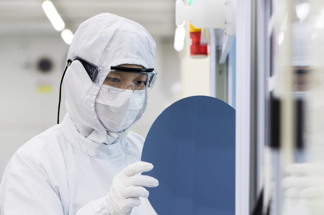
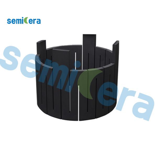
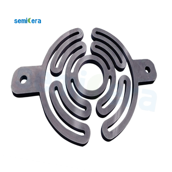
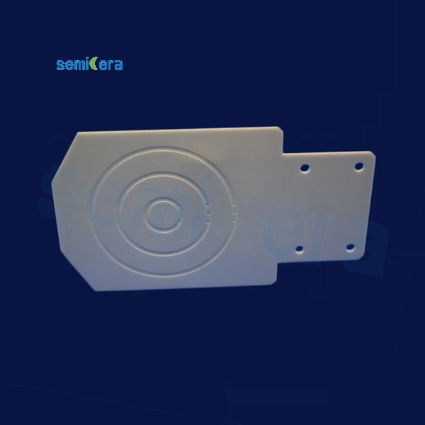
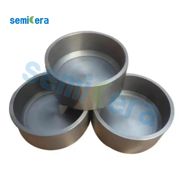
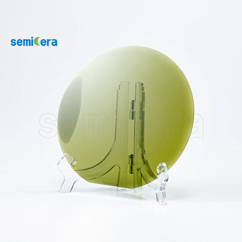
Semicera energy can provide customers with high-quality Conductive (Conductive), Semi-insulating (Semi-insulating), HPSI (High Purity semi-insulating) silicon carbide substrate; In addition, we can provide customers with homogeneous and heterogeneous silicon carbide epitaxial sheets; We can also customize the epitaxial sheet according to the specific needs of customers, and there is no minimum order quantity.
|
Items |
Production |
Research |
Dummy |
|
Crystal Parameters |
|||
|
Polytype |
4H |
||
|
Surface orientation error |
<11-20 >4±0.15° |
||
|
Electrical Parameters |
|||
|
Dopant |
n-type Nitrogen |
||
|
Resistivity |
0.015-0.025ohm·cm |
||
|
Mechanical Parameters |
|||
|
Diameter |
99.5 - 100mm |
||
|
Thickness |
350±25 μm |
||
|
Primary flat orientation |
[1-100]±5° |
||
|
Primary flat length |
32.5±1.5mm |
||
|
Secondary flat position |
90° CW from primary flat ±5°. silicon face up |
||
|
Secondary flat length |
18±1.5mm |
||
|
TTV |
≤5 μm |
≤10 μm |
≤20 μm |
|
LTV |
≤2 μm(5mm*5mm) |
≤5 μm(5mm*5mm) |
NA |
|
Bow |
-15μm ~ 15μm |
-35μm ~ 35μm |
-45μm ~ 45μm |
|
Warp |
≤20 μm |
≤45 μm |
≤50 μm |
|
Front(Si-face) roughness(AFM) |
Ra≤0.2nm (5μm*5μm) |
||
|
Structure |
|||
|
Micropipe density |
≤1 ea/cm2 |
≤5 ea/cm2 |
≤10 ea/cm2 |
|
Metal impurities |
≤5E10atoms/cm2 |
NA |
|
|
BPD |
≤1500 ea/cm2 |
≤3000 ea/cm2 |
NA |
|
TSD |
≤500 ea/cm2 |
≤1000 ea/cm2 |
NA |
|
Front Quality |
|||
|
Front |
Si |
||
|
Surface finish |
Si-face CMP |
||
|
Particles |
≤60ea/wafer (size≥0.3μm) |
NA |
|
|
Scratches |
≤2ea/mm. Cumulative length ≤Diameter |
Cumulative length≤2*Diameter |
NA |
|
Orange peel/pits/stains/striations/ cracks/contamination |
None |
NA |
|
|
Edge chips/indents/fracture/hex plates |
None |
NA |
|
|
Polytype areas |
None |
Cumulative area≤20% |
Cumulative area≤30% |
|
Front laser marking |
None |
||
|
Back Quality |
|||
|
Back finish |
C-face CMP |
||
|
Scratches |
≤5ea/mm,Cumulative length≤2*Diameter |
NA |
|
|
Back defects (edge chips/indents) |
None |
||
|
Back roughness |
Ra≤0.2nm (5μm*5μm) |
||
|
Back laser marking |
1 mm (from top edge) |
||
|
Edge |
|||
|
Edge |
Chamfer |
||
|
Packaging |
|||
|
Packaging |
The inner bag is filled with nitrogen and the outer bag is vacuumed. Multi-wafer cassette, epi-ready. |
||
|
*Notes: "NA" means no request Items not mentioned may refer to SEMI-STD. |
|||