Silicon carbide (SiC) single crystal material has a large band gap width (~Si 3 times), high thermal conductivity (~Si 3.3 times or GaAs 10 times), high electron saturation migration rate (~Si 2.5 times), high breakdown electric field (~Si 10 times or GaAs 5 times) and other outstanding characteristics.
The third generation semiconductor materials mainly include SiC, GaN, diamond, etc., because its band gap width (Eg) is greater than or equal to 2.3 electron volts (eV), also known as wide band gap semiconductor materials. Compared with the first and second generation semiconductor materials, the third generation semiconductor materials have the advantages of high thermal conductivity, high breakdown electric field, high saturated electron migration rate and high bonding energy, which can meet the new requirements of modern electronic technology for high temperature, high power, high pressure, high frequency and radiation resistance and other harsh conditions. It has important application prospects in the fields of national defense, aviation, aerospace, oil exploration, optical storage, etc., and can reduce energy loss by more than 50% in many strategic industries such as broadband communications, solar energy, automobile manufacturing, semiconductor lighting, and smart grid, and can reduce equipment volume by more than 75%, which is of milestone significance for the development of human science and technology.
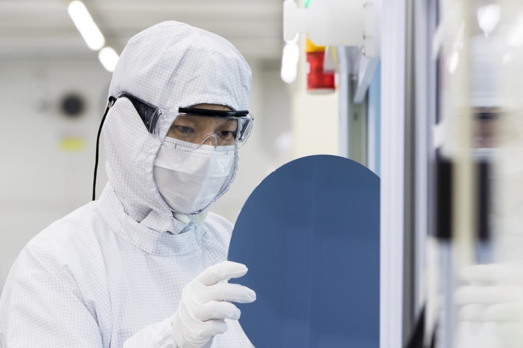
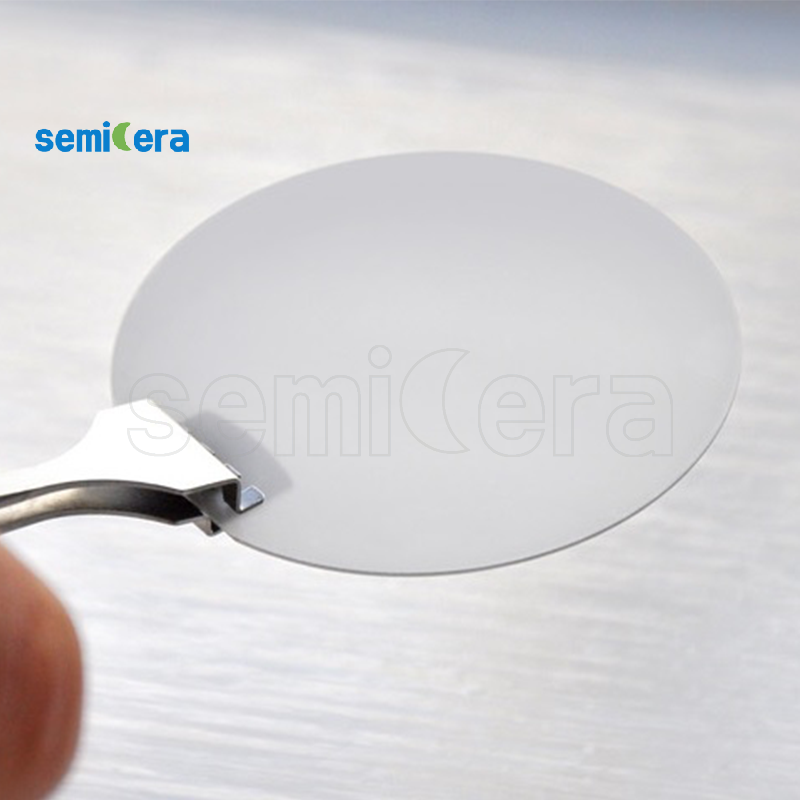
Semicera energy can provide customers with high-quality Conductive (Conductive), Semi-insulating (Semi-insulating), HPSI (High Purity semi-insulating) silicon carbide substrate; In addition, we can provide customers with homogeneous and heterogeneous silicon carbide epitaxial sheets; We can also customize the epitaxial sheet according to the specific needs of customers, and there is no minimum order quantity.
|
Items |
Production |
Research |
Dummy |
|
Crystal Parameters |
|||
|
Polytype |
4H |
||
|
Surface orientation error |
<11-20 >4±0.15° |
||
|
Electrical Parameters |
|||
|
Dopant |
n-type Nitrogen |
||
|
Resistivity |
0.015-0.025ohm·cm |
||
|
Mechanical Parameters |
|||
|
Diameter |
150.0±0.2mm |
||
|
Thickness |
350±25 μm |
||
|
Primary flat orientation |
[1-100]±5° |
||
|
Primary flat length |
47.5±1.5mm |
||
|
Secondary flat |
None |
||
|
TTV |
≤5 μm |
≤10 μm |
≤15 μm |
|
LTV |
≤3 μm(5mm*5mm) |
≤5 μm(5mm*5mm) |
≤10 μm(5mm*5mm) |
|
Bow |
-15μm ~ 15μm |
-35μm ~ 35μm |
-45μm ~ 45μm |
|
Warp |
≤35 μm |
≤45 μm |
≤55 μm |
|
Front(Si-face) roughness(AFM) |
Ra≤0.2nm (5μm*5μm) |
||
|
Structure |
|||
|
Micropipe density |
<1 ea/cm2 |
<10 ea/cm2 |
<15 ea/cm2 |
|
Metal impurities |
≤5E10atoms/cm2 |
NA |
|
|
BPD |
≤1500 ea/cm2 |
≤3000 ea/cm2 |
NA |
|
TSD |
≤500 ea/cm2 |
≤1000 ea/cm2 |
NA |
|
Front Quality |
|||
|
Front |
Si |
||
|
Surface finish |
Si-face CMP |
||
|
Particles |
≤60ea/wafer (size≥0.3μm) |
NA |
|
|
Scratches |
≤5ea/mm. Cumulative length ≤Diameter |
Cumulative length≤2*Diameter |
NA |
|
Orange peel/pits/stains/striations/ cracks/contamination |
None |
NA |
|
|
Edge chips/indents/fracture/hex plates |
None |
||
|
Polytype areas |
None |
Cumulative area≤20% |
Cumulative area≤30% |
|
Front laser marking |
None |
||
|
Back Quality |
|||
|
Back finish |
C-face CMP |
||
|
Scratches |
≤5ea/mm,Cumulative length≤2*Diameter |
NA |
|
|
Back defects (edge chips/indents) |
None |
||
|
Back roughness |
Ra≤0.2nm (5μm*5μm) |
||
|
Back laser marking |
1 mm (from top edge) |
||
|
Edge |
|||
|
Edge |
Chamfer |
||
|
Packaging |
|||
|
Packaging |
Epi-ready with vacuum packaging Multi-wafer cassette packaging |
||
|
*Notes: "NA" means no request Items not mentioned may refer to SEMI-STD. |
|||