SiC wafer carriers, as key consumables in the third-generation semiconductor industry chain, their technical characteristics directly affect the yield of epitaxial growth and device manufacturing. With the surging demand for high-voltage and high-temperature devices in industries such as 5G base stations and new energy vehicles, the research and application of SiC wafer carriers are now facing significant development opportunities.
In the field of semiconductor manufacturing, silicon carbide wafer carriers mainly undertake the important function of carrying and transmitting wafers in epitaxial equipment. Compared with traditional quartz carriers, SiC carriers exhibit three core advantages: Firstly, their coefficient of thermal expansion (4.0×10^-6/℃) is highly matched with that of SiC wafers (4.2×10^-6/℃), effectively reducing thermal stress in high-temperature processes; Secondly, the purity of high-purity SiC carriers prepared by the chemical vapor deposition (CVD) method can reach 99.9995%, avoiding the common sodium ion contamination problem of quartz carriers. Furthermore, the melting point of SiC material at 2830℃ enables it to adapt to the long-term working environment above 1600℃ in MOCVD equipment.
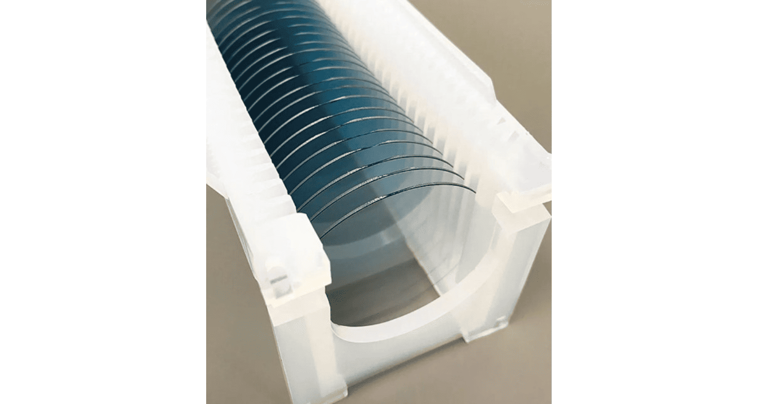
At present, the mainstream products adopt a 6-inch specification, with a thickness controlled within the range of 20-30mm and a surface roughness requirement of less than 0.5μm. To enhance the epitaxial uniformity, leading manufacturers construct specific topological structures on the carrier surface through CNC machining. For instance, the honeycomb-shaped groove design developed by Semiceri can control the thickness fluctuation of the epitaxial layer within ±3%. In terms of coating technology, the TaC/TaSi2 composite coating can extend the service life of the carrier to over 800 times, which is three times longer than that of the uncoated product.
At the industrial application level, SiC carriers have gradually permeated the entire manufacturing process of silicon carbide power devices. In the production of SBD diodes, the use of SiC carriers can reduce the epitaxial defect density to less than 0.5cm ². For MOSFET devices, their excellent temperature uniformity helps to increase the channel mobility by 15% to 20%. According to industry statistics, the global SiC carrier market size exceeded 230 million US dollars in 2024, with a compound annual growth rate maintained at around 28%.
However, technical bottlenecks still exist. The warpage control of large-sized carriers remains a challenge – the flatness tolerance of 8-inch carriers needs to be compressed to within 50μm. At present, Semicera is one of the few domestic companies that can control warping. Domestic enterprises such as Tianke Heda have achieved mass production of 6-inch carriers. Semicera is currently assisting Tianke Heda in customizing SiC carriers for them. At present, it has approached international giants in terms of coating processes and defect control. In the future, with the maturity of heteroepitaxy technology, dedicated carriers for GaN-on-SiC applications will become a new research and development direction.
Post time: Jun-06-2025