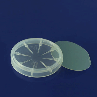
Gallium nitride (GaN) developed relatively late. It uses hydride vapor deposition technology to deposit large-area gallium nitride films on the surface of sapphire substrates. Gallium nitride features a large bandgap width, high breakdown voltage, high thermal conductivity, high saturation electron drift velocity and strong radiation resistance. It is the material with the highest theoretical electro-optical and photoelectric conversion efficiency to date. The main epitaxial growth methods of gallium nitride include metal-organic chemical vapor deposition (MOCVD), hydride vapor deposition (HVPE), and molecular beam epitaxy (MBE).
At present, apart from MOCVD, MBE molecular beam epitaxy has also become an important growth method for semiconductor materials such as gallium nitride. MBE is an epitaxial growth method for growing high-quality crystal films on substrate surfaces, but it needs to be carried out in a high vacuum or even ultra-high vacuum environment. The advantages of MBE are as follows: Although the growth rate of MBE usually does not exceed 1 micrometer per hour, which is equivalent to the growth of only one single-atom layer per second or longer, it is easy to achieve precise control over film thickness, structure and composition, and it is easy to realize heterogeneous structures and quantum structures with steep interfaces, etc. The low epitaxial growth temperature reduces the lattice defects introduced at the interface due to different thermal expansion coefficients. Compared with the chemical processes of HVPE and MOCVD, MBE is a physical deposition process, so the impurity pollution caused by chemical reactions is not taken into account.
Doping process is a key step that determines the performance of devices. Silane gas, as an N-type doping source, needs to have its concentration gradient precisely controlled between 10 to the power of 17 and 10 to the power of 19 per cubic centimeter. During this process, the electron mobility must reach over 300 square centimeters per volt-second to be considered qualified. The preparation of quantum well structures poses a greater challenge to the technological level. The growth temperature of InGaN/GaN multi-quantum Wells needs to be reduced to 780 to 850 degrees Celsius, and the thickness of the well layers should be controlled at the nanometer level. Any deviation will affect the luminescence characteristics of the final device.
In the later stage of the process, dry etching adopts inductively coupled plasma technology, and the mixed gas of chlorine and boron trichloride used needs to be precisely proportioned. The etching rate should be controlled at 200 to 300 nanometers per minute, and the side wall Angle should be maintained within a range of ± two degrees of 85 degrees. When making ohmic contact, the selection of the metal stacking layer and the annealing conditions directly affect the contact resistance, which is usually required to be controlled below 0.5 ohms per millimeter. The final passivation layer deposition is carried out by plasma-enhanced chemical vapor deposition. Both the refractive index and stress of the film need to be strictly monitored. Throughout the entire process flow, the quality inspection stage is indispensable. Detection methods such as X-ray diffraction and photoluminescence spectroscopy ensure that each stage meets the design standards.
Post time: Jul-09-2025

