In modern integrated circuit and power device manufacturing, the silicon epitaxy process has become one of the fundamental key technologies. Silicon epitaxy refers to the growth of a single-crystal silicon film on the surface of a single-crystal silicon substrate, with crystal orientation and lattice continuity consistent with the substrate. The thickness, doping type and concentration, as well as defect level of this epitaxial layer can all be precisely engineered as required, and are used to construct the active regions of devices or electric-field control regions.
I. Overview of Process Principles
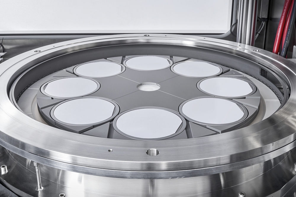
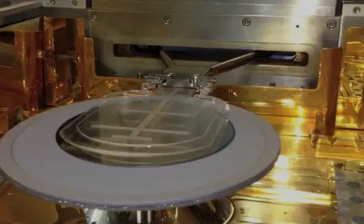
Silicon epitaxy is typically realized by chemical vapor deposition (CVD). During the process, thoroughly cleaned single-crystal silicon wafers are placed in a high-temperature reaction chamber, and silicon-containing precursor gases (such as SiH₄, SiH₂Cl₂, etc.) are introduced under a hydrogen atmosphere. Within a temperature range of approximately 900–1200 ℃, the precursors decompose at the silicon surface, releasing silicon atoms. Under the “template” effect of the substrate crystal lattice, these atoms rearrange according to the existing crystal orientation, forming an epitaxial single-crystal layer with the same orientation as the substrate, rather than a polycrystalline or amorphous structure.
Prior to epitaxial growth, surface preparation is crucial. The silicon wafers must undergo multiple wet cleaning steps to remove organic residues, metallic impurities, and particles, and the surface is refreshed by controlled oxidation/deoxidation steps. After entering the reaction chamber, a high-temperature hydrogen bake is usually performed to remove the very thin native oxide layer and to smooth the surface. Only when the surface is clean and the lattice is intact can a high-quality epitaxial layer with low defect density be obtained.
II. Doping and Structural Control
During epitaxial growth, gases containing dopant species such as PH₃ (phosphorus), B₂H₆ (boron), and AsH₃ (arsenic) can be introduced simultaneously to achieve in-situ doping. By adjusting the dopant gas flow rates, chamber pressure, and temperature, different concentration gradients and junction structures can be formed along the thickness direction, enabling various combinations from lightly doped drift regions to heavily doped collector regions. This provides a multi-level design space for high-voltage devices, analog circuits, and power chips.
In addition, process variants such as selective epitaxy (SEG) and low-temperature epitaxy can be employed. SEG is used to grow epitaxial layers only on exposed silicon regions, for example to form raised source/drain regions or strained Si/SiGe structures; low-temperature epitaxy is used in the later stages of device fabrication to reduce thermal budget and avoid adverse impact on existing fine structures.
III. Advantages of Silicon Epitaxy Technology in Device Manufacturing
-
Reduction of series resistance and simplification of isolation structures
By growing epitaxial layers with specified doping and thickness on the substrate surface, the current conduction path can be optimized and the series resistance of the device reduced. At the same time, the epitaxial layer facilitates the formation of more effective isolation structures, weakening the coupling of parasitic devices. This simplifies isolation design in CMOS processes, reduces parasitic silicon-controlled rectifier (SCR) effects and latch-up phenomena, and enhances circuit stability and reliability. -
Flexible stacking of layers with different resistivities
The epitaxial process allows a high-resistivity epitaxial layer to be grown on a low-resistivity substrate, or a low-resistivity epitaxial layer to be grown on a high-resistivity substrate, thus enabling multi-layer structures with different resistivities on the same wafer. Through this “free combination” of high/low resistivity layers, the electric-field distribution and conduction path can be designed more precisely, meeting the diverse electrical requirements of high-voltage devices, analog circuits, and power devices. -
Direct formation of high-quality PN junctions and avoidance of compensation effects
Using silicon epitaxy, an N-type epitaxial layer can be grown on a P-type substrate, or a P-type epitaxial layer on an N-type substrate, so that a PN junction is formed directly at the interface. This “hetero-epitaxy” approach does not rely on conventional diffusion or ion implantation to form junction regions inside the single-crystal substrate, and effectively avoids the compensation effects commonly encountered in diffusion doping. It is conducive to obtaining PN junctions with controllable junction depth, well-defined junction profiles, and stable electrical characteristics. -
Selective epitaxy with masks, enabling integration of complex structures
When epitaxy is combined with mask processes, selective epitaxial growth can be realized only in regions where bare silicon is exposed, while growth does not occur or is negligible in regions covered by dielectric materials such as silicon dioxide or silicon nitride. This characteristic provides a practical route for forming locally raised source/drain regions, strain regions, and three-dimensional structures, as well as for fabricating special-purpose integrated circuits, thereby creating favorable conditions for the design of complex device structures and differentiated product platforms. -
Highly controllable doping type and concentration distribution
During epitaxial growth, the type and flow rate of dopant gases can be adjusted in real time according to device requirements, enabling precise control of the doping type (P-type or N-type) and concentration level in the epitaxial layer. The variation of dopant concentration along the thickness direction can be designed either as an abrupt interface (forming a distinct PN junction or resistivity step) or as a gradual profile (realizing smooth electric fields or buffer layer structures). This flexible control over the doping profile allows more refined trade-offs among key parameters such as breakdown voltage, on-resistance, and junction capacitance.
Post time: Nov-26-2025