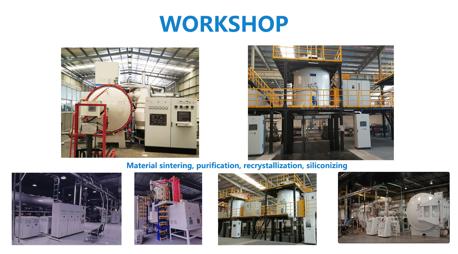
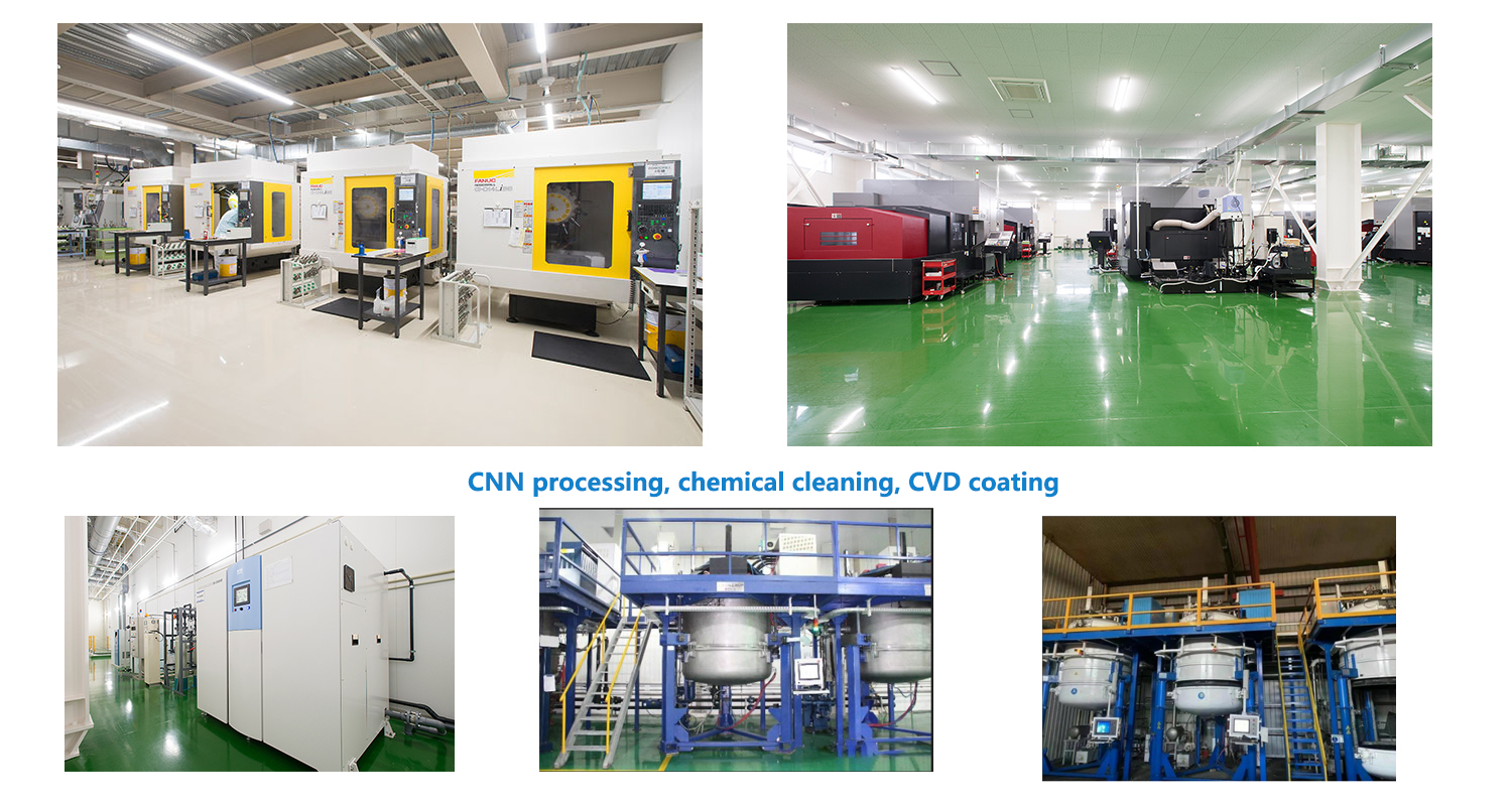
In advanced epitaxial devices such as ASM, 12-inch silicon carbide (SiC) coated bases (susceptor) are becoming key consumables in the manufacturing of third-generation semiconductors.
The traditional graphite base faces two major challenges in the high-temperature MOCVD process: one is the contamination caused by the reverse diffusion of silicon vapor, and the other is the cracking caused by the difference in thermal expansion coefficients. The β-SiC coating fabricated by chemical vapor deposition (CVD) process, with its dense structure of 4.3g/cm³ and thermal conductivity of 3.2W/m·K, can still maintain a flatness of ±0.2mm at 1600 ° C. Test data from ASML of the Netherlands shows that the base coated with high-quality SiC can reduce the wafer bow from 120μm to below 35μm.
To meet the epitaxial requirements of 12-inch wafers, modern bases adopt gradient coating technology: the bottom layer is a 50μm buffer layer (SiC+10%TiC), the middle layer is 120μm high-purity SiC, and the surface is polished by plasma to achieve a mirror-like effect with Ra<0.05μm. This structure keeps the temperature uniformity within ±1.5 ° C (measured data from the EPI Centura platform of Applied Materials). It is worth noting that the multi-pore channel design on the back of the base achieves uniform distribution of hydrogen carrier gas, reducing the fluctuation of epitaxial growth rate to ±1.2%.


