
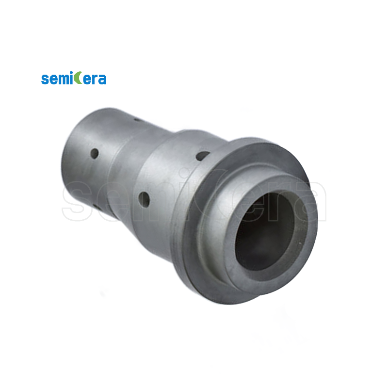
The AMAT 12" Insert Ring is installed around the wafer processing region inside plasma chambers, typically in etch and PVD systems. It is designed specifically for 300 mm wafer platforms, where precise plasma control is essential for advanced semiconductor manufacturing.
Key Product Information
|
Item |
Description |
|
Product Name |
Insert Ring |
|
Part Number |
0200-01797 |
|
Wafer Size |
300 mm (12 inch) |
|
Component Type |
Plasma Control Ring / Insert Ring |
|
Application |
Etch / PVD / Plasma Processing |
|
Installation Position |
Wafer Edge / ESC Periphery |
|
Supplier |
Semicera Semiconductor |
Material Characteristics
The AMAT 12" INSERT RING 0200-01797 is typically manufactured using advanced semiconductor-grade materials, selected based on process requirements and performance targets.
Common Material Options
Silicon (Si)
Widely used in etch environments due to its compatibility with silicon wafers. It minimizes contamination and provides excellent resistance to plasma erosion.
High-Purity Quartz (SiO₂)
Used in applications requiring electrical insulation and ultra-low contamination. Quartz offers strong chemical stability and plasma resistance.
Advanced Ceramics (e.g., Al₂O₃, Y₂O₃-coated materials)
Provide enhanced durability, superior corrosion resistance, and extended lifetime in aggressive plasma conditions.
Key Material Advantages
Low Contamination Risk
Semiconductor-grade materials ensure minimal impurity introduction, supporting high-yield wafer production.
Excellent Plasma Resistance
Materials are selected to withstand ion bombardment, reactive gases, and high-energy plasma exposure.
Thermal Stability
Maintains structural integrity under high temperatures and thermal cycling.
Electrical Performance
Supports stable RF fields and plasma conditions through insulating or controlled conductive properties.
-

Mirror SIC mirror silicon carbide ceramic mirro...
-

High purity SiC ceramic reflector can be custom...
-
Silicon Carbide Nozzles for Sulfuric Acid Atomizer
-

SiC products high temperature resistant SiC cer...
-
High Wear Resistance Silicon Carbide Ceramic Li...
-
SIC press-free sintered silicon carbide ceramic...