
Core Summary: A Dutch optical research spin-off commissioned 10 custom rectangular silicon wafers, 29.2mm × 70mm, 230µm thick, initially requesting 0.1nm surface roughness with zero edge chipping after cutting. After evaluation, the technical team determined these two specifications could not realistically be achieved together, and was upfront with the customer about what was actually achievable — roughness <0.2nm RMS with chipping kept to a minimal, controlled range. The customer confirmed and placed the order on this basis, and all 10 wafers were ultimately delivered meeting this standard, with no misunderstanding or delivery dispute throughout.
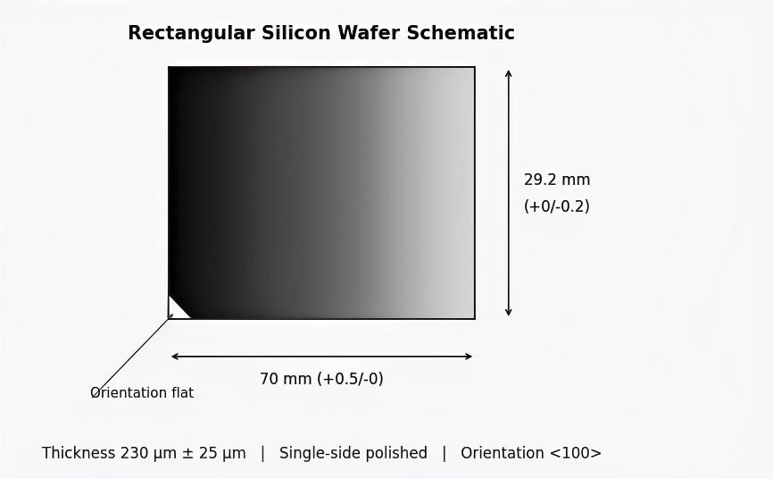
Overview
Industry: Optical research and precision optical systems development Process: Secondary cutting of silicon wafers (custom rectangular small-size wafers cut from our own wafer stock)
Solution: Transparent communication on the process boundaries of chipping and roughness, single-side polishing optimization, achieving <0.2nm surface roughness
Services: Custom cutting, single-side polishing, roughness inspection, individual protective packaging Results: All 10 rectangular silicon wafers delivered meeting the <0.2nm roughness standard
A Dutch optical research spin-off requested 10 single-side polished rectangular silicon wafers, 29.2mm × 70mm, thickness 230µm ± 25µm, to be obtained via secondary cutting, with a clearly stated requirement of approximately 0.1nm RMS surface roughness and no edge chipping after cutting. After evaluation, the technical team confirmed that cutting inevitably affects the edges, and that 0.1nm roughness — a specification typical of as-polished, uncut wafers — could not be achieved; a stable, realistically achievable roughness was <0.2nm RMS. Rather than avoiding the gap, the team communicated the actual process boundaries to the customer. Both sides confirmed; the customer accepted the <0.2nm standard, and placed the order; all 10 wafers were ultimately delivered to this standard.
Core Conclusion: The customer's initial targets were 0.1nm roughness and zero chipping; based on process realities, the team adjusted this to <0.2nm roughness with controlled chipping, and all 10 wafers were ultimately delivered meeting the adjusted standard.
Customer Background: Why Would an Optics Research Company Need Small Silicon Wafers?
This optical research spin-off focuses on R&D related to precision optical systems and detectors, and required 10 rectangular silicon wafers measuring 29.2mm × 70mm, 230µm thick, single-side polished, <100> orientation, obtained via secondary cutting from existing wafer stock. Upon confirmation, the customer did not actually have existing wafers on hand, so the cutting needed to be performed on wafers we produced in-house. This kind of non-standard rectangular small-size cutting is a typical "non-mainstream" requirement — wafers on the general market are mostly standard round wafers, while optical R&D companies often need materials in specific sizes that match their own module structures.
Core Conclusion: Optical R&D companies' wafer size requirements are highly customized; standard round wafers cannot meet their module structure needs, making secondary-cut custom rectangular small-size silicon wafers a hard requirement.
Challenge: Can Edge Chipping Be Completely Avoided?
Core Conclusion: The 0.1nm roughness and zero-chipping requirements are inherently in conflict for the cutting process; the team chose to first verify internal process capability and be upfront with the customer, rather than blindly accepting the order and promising the original specs.
Placing a 0.1nm RMS surface roughness requirement alongside a zero-chipping-edge requirement creates a real conflict for the cutting process. Cutting is a mechanical stress process, and edges will inevitably develop microscopic chipping — achieving completely zero chipping is very difficult industry-wide. Meanwhile, 0.1nm RMS is a specification typical of as-polished wafers; after secondary cutting, the surface roughness that can be stably achieved is generally on the order of 0.2nm. Promising to deliver against the customer's original specs outright risked being unable to fulfill the order, or repeated rework and extended lead times. The technical team therefore first validated internal process capability rather than accepting the order outright.
Solution: Roughness Control and Transparent Communication
Core Conclusion: Stabilizing roughness at <0.2nm RMS and reducing chipping to a minimal range through parameter optimization, combined with transparent communication in place of vague promises, was the key to this case's smooth execution.
After internal verification, the team concluded: chipping cannot be reduced to zero, but can be controlled to a very small range through parameter optimization; roughness cannot reach 0.1nm, but can be stably achieved at <0.2nm RMS. The team communicated the actual situation, along with the reasons for the process limitations, fully and directly to the customer — rather than being vague or accepting the order first and explaining later. For an R&D customer, the boundaries of material performance directly determine whether subsequent experiments and designs are feasible, so clarifying this upfront matters more than explaining it after the fact.
|
Metric |
Customer's Initial Requirement |
Actual Delivered Level |
|
Surface roughness |
~0.1 nm RMS |
<0.2 nm RMS |
|
Cut edge |
No chipping |
Chipping controlled to a minimal range, not zero chipping |
|
Size / Thickness |
29.2mm × 70mm, thickness 230µm ± 25µm |
Meets tolerance requirements |
After confirming the comparison, the customer formally placed the order. The team completed cutting and polishing of 10 wafers from our existing wafer stock, with each wafer individually packaged in a clean protective case, ensuring every piece the customer received retained the actual inspected condition at the time of cutting.

Figure 2: Illustration of the surface roughness inspection report for the cut rectangular silicon wafer, measured value below 0.2nm RMS
Results: All 10 Rectangular Silicon Wafers Delivered Meeting the <0.2nm Standard
Core Conclusion: All 10 wafers were delivered meeting the adjusted <0.2nm standard, individual protective packaging ensured transport safety, and the customer expressed satisfaction with the communication throughout.
- Quantity delivered: 10 pieces, 29.2mm × 70mm, thickness 230µm, single-side polished, <100> orientation
- Surface roughness: Measured stably below 0.2nm RMS
- Chipping: Controlled to an acceptable minimal range
- Packaging: Each piece individually protectively packaged to ensure transport safety
- Communication process: The customer was fully informed of the actual process level throughout, with no misunderstanding of specifications or delivery disputes
Conclusion: Key Process Considerations for Custom-Cutting Silicon Wafers from Existing Stock
The value of custom silicon wafers lies not in "whether the target size can be cut," but in whether the real process boundaries of chipping and roughness can be clearly communicated upfront. In secondary-cut customization of silicon wafers as well as compound semiconductor wafers such as SiC and GaAs, what truly determines success is often: honest evaluation of process boundaries, transparent communication about chipping and roughness, and inspection plus individual packaging to safeguard delivery quality. If you need custom-cut rectangular, irregular, or non-standard-size silicon wafers based on existing wafer stock, send us your target size, thickness, crystal orientation, and roughness requirements — we will first assess the realistically achievable specifications, clearly explain chipping risk and roughness levels, then quote, and inspect each wafer individually before delivery.
Post time: Aug-22-2026