
Amidst the explosive growth of nanoscale semiconductor manufacturing and compound semiconductors (such as SiC and GaN), there exists an often-overlooked “unsung hero” that determines chip yield and equipment lifespan: the Chemical Vapor Deposition (CVD) coating process.
CVD coating plays an indispensable role in everything from the fabrication of micron- and nanoscale interconnects and dielectric layers within chips to the protection of graphite susceptors and components that support chip growth at temperatures exceeding 1,000°C. Drawing upon the theoretical framework established by Jan-Otto Carlsson and Peter M. Martin in their seminal review *Chemical Vapour Deposition: An Overview*, and integrating semiconductor manufacturing practices with technologies from industry leaders like Semicera Semiconductor, this article offers a systematic exploration of the fascinating world of CVD coating.
I. What is the CVD Coating Process?
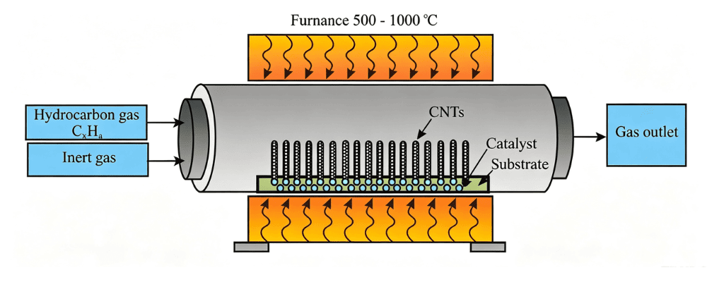
Simply put, CVD (Chemical Vapor Deposition) coating is a technique that utilizes gas-phase chemical reactions to synthesize and deposit solid thin films or coatings onto a substrate surface.
Within the classic theoretical framework established by Carlsson and Martin, CVD is defined as a complex system involving the synergistic interaction of thermodynamic equilibrium, fluid dynamic transport, and surface chemical kinetics.
At the microscopic level, the complete CVD coating reaction process can be broken down into five core steps:
1. Precursor Transport: Reactant gases (precursors) and carrier gases are introduced into the reaction chamber and transported via diffusion through the fluid boundary layer to the substrate surface (e.g., silicon wafers or graphite susceptors);
2. Gas-Phase/Surface Adsorption: Precursor molecules undergo homogeneous reactions in the gas phase or undergo direct physical/chemical adsorption onto the substrate surface;
3. Surface Chemical Reactions: Activated by thermal energy, plasma, or light, the adsorbed molecules undergo heterogeneous reactions, forming solid film nuclei that gradually grow into a continuous film;
4. By-product Desorption: Gaseous by-products generated by the reaction desorb from the surface;
5. Exhaust: Unreacted residual gases and by-products are evacuated from the chamber by a vacuum pump.
II. Comparative Overview of Variants: A Comparison of Major CVD Methods
As noted by Carlsson and Martin, CVD has spawned a wide array of technical branches to accommodate varying requirements regarding material thermal sensitivity, thickness uniformity, and microstructure. The following is a comparative overview of the key CVD technologies used in semiconductor manufacturing:
|
CVD Technology Type |
Activation Energy Source |
Typical Operating Pressure / Temperature |
Key Advantages (Pros) |
|
APCVD (Atmospheric Pressure CVD) |
Thermal energy only Atmospheric pressure (1 atm) |
Atmospheric pressure (1 atm): 300 – 500°C |
High deposition rate; relatively simple equipment structure |
|
LPCVD (Low-Pressure CVD) |
Thermal energy only |
Low pressure (10–100 Pa); 550–900°C |
Rapid gas diffusion; extremely dense films; excellent step coverage |
|
PECVD (Plasma-Enhanced CVD) |
Plasma (RF/Microwave) + |
Thermal energy Low pressure (10–500 Pa); 100–400°C |
Low thermal budget ; high deposition rate |
|
MOCVD (Metal-Organic CVD) |
Thermal energy / Light |
Atmospheric/Low pressure; 400–1200°C |
Precise control of ultra-thin single-crystal epitaxy; capable of growing complex multi-component compounds |
|
ALD (Atomic Layer Deposition) |
Thermal energy / Plasma |
Low pressure; 100–400°C |
Self-limiting reaction; alternating single-atomic-layer growth; near-100% conformality |
III. Selection of Coating Method: Comparison of CVD with Other Coating Technologies
In the field of industrial coatings, common techniques—in addition to CVD—include PVD (Physical Vapor Deposition, such as sputtering and evaporation), thermal spraying, and sol-gel. Why does CVD hold a dominant position in semiconductor and high-precision manufacturing?
|
Surface Coating Technologies (Coatings) |
Physical evaporation/sputtering |
Highly directional; suitable for flat surfaces or low aspect ratios |
|
Thermal Spray: Mechanical bonding |
Thick films/rough surfaces; lower bond strength |
|
|
CVD (Chemical): Gas-phase chemical reaction |
Non-directional/highly conformal; strong chemical bonding; suitable for ultra-pure applications or complex 3D structures |
1. Comparison with PVD (Physical Vapor Deposition):
Conformality & Step Coverage: PVD is a “line-of-sight” process; it performs poorly when depositing on the sidewalls or backsides of deep holes, high-aspect-ratio trenches, and complex 3D components. In contrast, CVD relies on gas diffusion and surface reactions, offering non-directional deposition capabilities that allow it to perfectly coat complex geometries.
Adhesion: CVD reactions typically occur at higher temperatures, facilitating atomic-level diffusion and chemical bonding at the film-substrate interface; this results in adhesion strength significantly superior to the physical adsorption characteristic of PVD.
2. Comparison with Thermal Spraying:
Density & Thickness Control: Thermal spraying is suitable for producing thick, coarse-grained coatings ranging from hundreds of microns to millimeters in thickness, but these coatings often exhibit high porosity. CVD, however, enables precise control over coating formation, yielding pore-free, highly dense coatings ranging from the nanometer scale to tens of microns in thickness.
3. Comparison with Sol-Gel:
Purity & Defects: While the sol-gel method is cost-effective, it is prone to shrinkage cracks caused by solvent evaporation during the annealing process. Conversely, CVD gas-phase precursors can be purified via distillation to ultra-high purity levels (6N–9N), resulting in extremely low defect rates.
IV. Practical Applications of CVD Coatings in Semiconductor Equipment Components
In the fields of semiconductor manufacturing and epitaxial growth, exposure to high temperatures, highly corrosive gases (such as HCl and NH₃), and plasma erosion is commonplace. Unprotected graphite or metal substrates are highly susceptible to particle shedding, decarburization, or corrosion, which can lead to catastrophic metal contamination of wafers.
Taking industry leader Semicera Semiconductor as an example, their ultra-pure coated components—developed using advanced CVD technology—effectively equip semiconductor equipment with “diamond-like armor”:
1. CVD SiC Coating (Silicon Carbide Coating)
Principles and Characteristics: Precursors such as methyltrichlorosilane (MTS) are decomposed at high temperatures to deposit a highly dense, high-purity (up to 99.99995%) β-SiC crystalline layer onto a graphite substrate. This coating features extreme hardness (~40 GPa), resistance to temperatures exceeding 1600°C, and excellent resistance to acid and alkali corrosion.
Representative Products (Semicera):
SiC-Coated Graphite Susceptor: Used in 8-inch and 12-inch silicon epitaxy and GaN-on-SiC epitaxy equipment (e.g., AMAT, ASM, and Aixtron platforms).
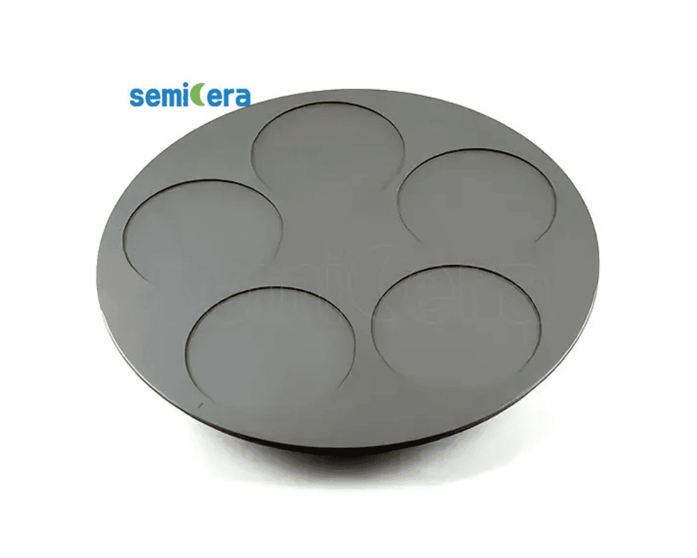
SiC Showerhead & Etch Plate: Used in ICP etching and PECVD chambers to ensure uniform gas distribution and resistance to plasma erosion.
2. CVD TaC Coating (Tantalum Carbide Coating)
Principles and Characteristics: Tantalum carbide (TaC) has a melting point approaching 3880°C. In environments exceeding 2000°C involving strong reducing or ammoniating conditions (such as ultra-high-temperature SiC single-crystal growth or GaN MOCVD processes), traditional SiC coatings may decompose, whereas CVD TaC coatings provide exceptional chemical stability.
Representative Products (Semicera)
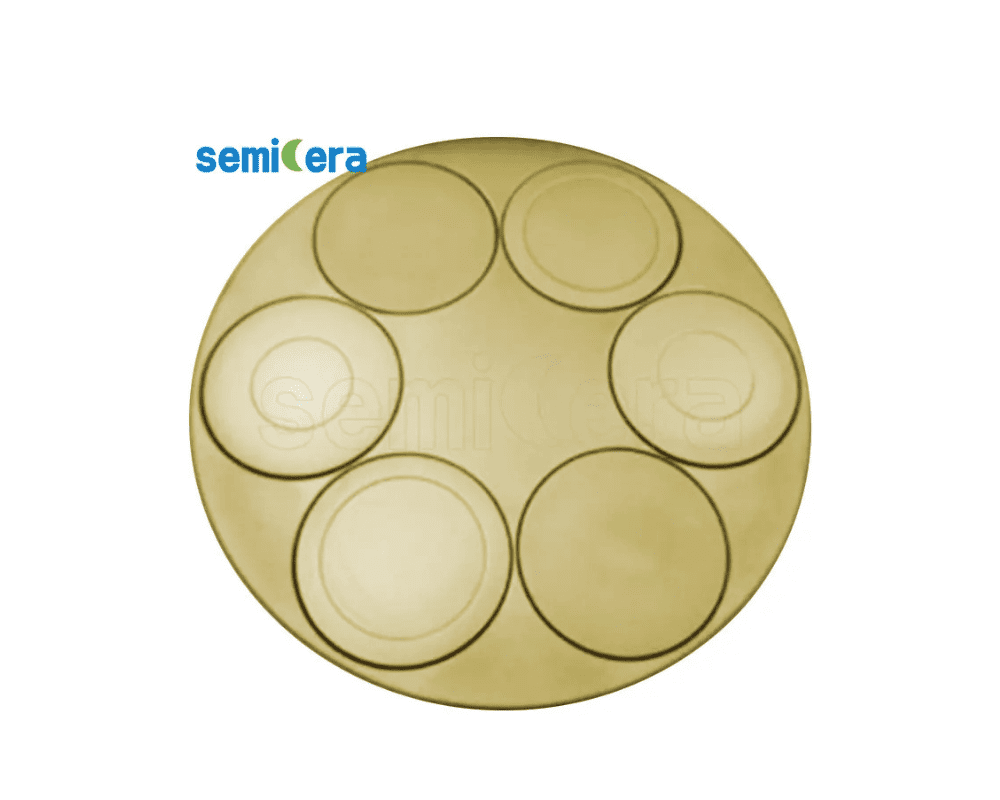
TaC-Coated MOCVD Heaters and Susceptors: Designed specifically for Deep-UV LEDs and high-temperature epitaxy of third-generation semiconductors.
TaC-Coated Guide Rings and Porous Graphite Components: Address issues regarding high-temperature volatilization and carbon contamination during single-crystal growth.
V. Challenges and Future Outlook
1. Current Physical Limit Challenges Facing the Industry
Void-free filling of structures with ultra-high aspect ratios (HAR): In the deep holes (with aspect ratios of hundreds-to-one) found in GAA transistors or 3D NAND devices, gas-phase precursors tend to deposit prematurely and clog the opening, leading to the formation of internal voids.
Thermal Budget and Thermal Stress Matching: Advanced process nodes are extremely sensitive to thermal budgets; furthermore, a mismatch in the Coefficient of Thermal Expansion (CTE) between the coating (e.g., SiC/TaC) and the substrate can easily trigger micro-cracking or peeling of the coating during high-temperature cycling (at temperatures around 1000°C).
Nanoscale Particles and Environmental Control: At nanoscale nodes, the deposition of even a few particles (sized at the nanometer level) generated via gas-phase nucleation can result in the scrapping of an entire wafer.
2. Future Trends
Precursor Molecular Engineering: With the introduction of new materials such as Ru, Co, HfO2, and La2O3, a key breakthrough lies in designing novel molecules that combine high volatility, low toxicity, and high thermal stability, while also enabling “Selective Area CVD.”
Low-Temperature Processing and Area-Selective CVD (ASCVD): By integrating PECVD, ALD, and Self-Assembled Monolayer (SAM) technologies, deposition can be confined to specific areas where it is required. This approach disrupts the traditional “blanket deposition plus etching” lithography workflow, thereby significantly reducing process costs. Multi-technology integration of CVD, PVD, and ALD: Future high-end semiconductor equipment will increasingly adopt hybrid deposition technologies (such as PE-ALD and plasma-assisted MOCVD), combining the respective strengths of these techniques to meet the processing requirements for extreme microstructures.
Post time: Aug-10-2026