
Ⅰ. Introduction
Modern semiconductor devices are becoming increasingly powerful, smaller, and more energy efficient. Behind many of these innovations is a highly sophisticated manufacturing technology that enables engineers to build semiconductor materials layer by layer at the atomic scale — Metal Organic Chemical Vapor Deposition (MOCVD).
From high-brightness LEDs and laser diodes to GaN power electronics and advanced compound semiconductor devices, MOCVD has become one of the most important epitaxial growth technologies in the semiconductor industry.
Ⅱ. How does MOCVD actually work?
In simple terms, MOCVD is a process that uses precisely controlled chemical reactions to transform gaseous metal-organic compounds into high-quality crystalline semiconductor films on a heated substrate.
Unlike traditional coating technologies, MOCVD does not simply deposit a thin layer onto a surface. Instead, it creates a new crystal structure by controlling how atoms arrange themselves during growth. This atomic-level control determines the final electrical, optical, and mechanical performance of semiconductor devices.
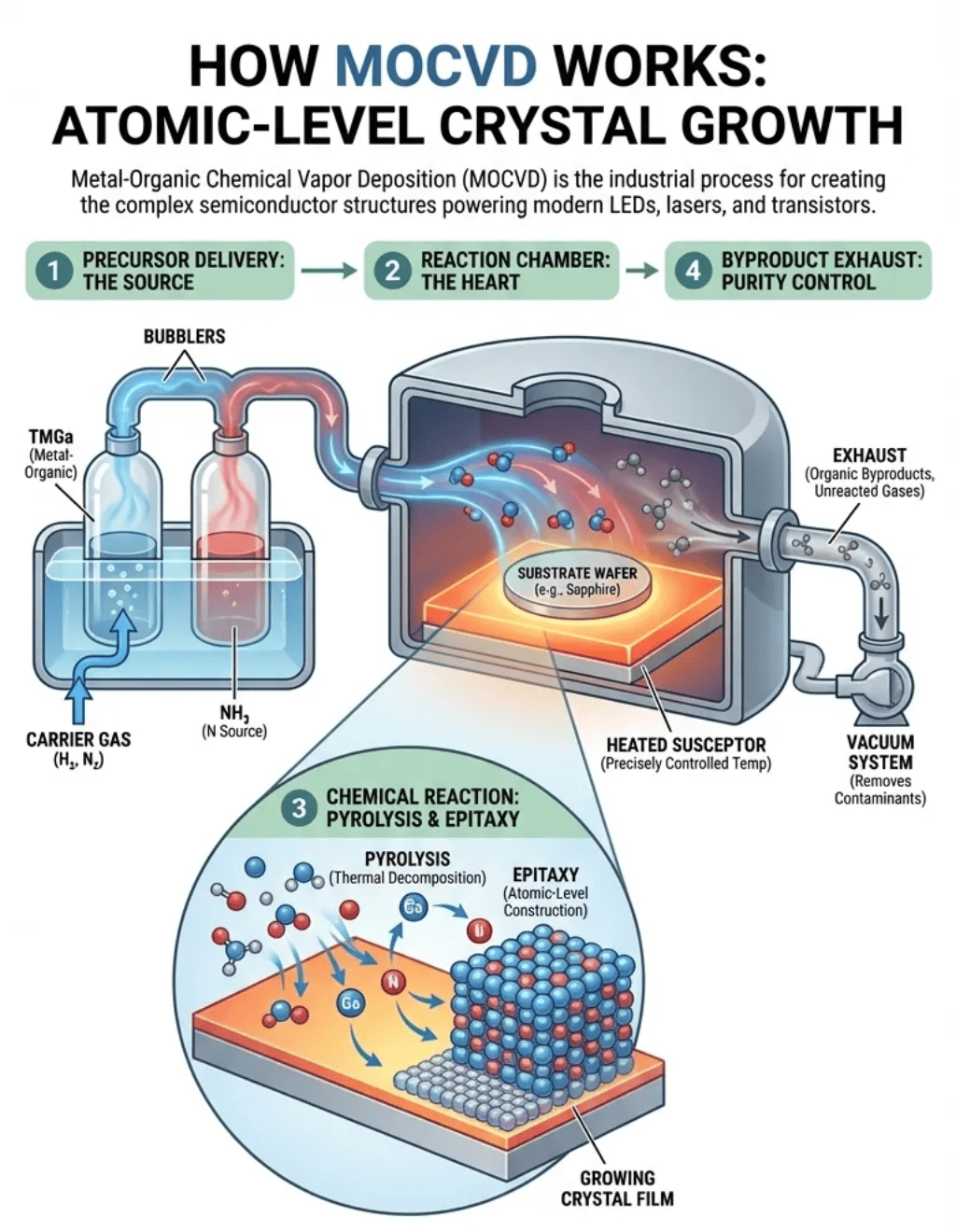
Ⅲ. The MOCVD Process: From Gas to Crystal
The fundamental concept behind MOCVD is relatively straightforward:
Precursors are delivered into a reactor → chemical reactions occur on a heated substrate → atoms form an epitaxial crystal layer.
However, achieving high-quality semiconductor films requires extremely precise control over every stage of this process.
Inside an MOCVD reactor, metal-organic precursor gases such as Trimethylgallium (TMGa), Trimethylaluminum (TMAl), and Trimethylindium (TMIn) are introduced together with reactive gases such as ammonia (NH₃).
These gases are transported into the reaction chamber through carefully designed gas delivery systems. Under high-temperature conditions, the precursor molecules decompose and release semiconductor atoms.
For example, during GaN epitaxy, gallium-containing precursors react with ammonia to form gallium nitride crystals on the wafer surface.
The overall process involves several key physical and chemical mechanisms:
- First, precursor molecules travel through the reactor chamber with precisely controlled gas flow.
- Second, these molecules reach the heated substrate surface and undergo thermal decomposition.
- Third, released atoms migrate across the surface and attach themselves to the growing crystal lattice.
- Finally, unwanted chemical by-products are removed through the exhaust system, leaving behind a high-quality epitaxial semiconductor layer.
The challenge is that semiconductor devices require extremely uniform and defect-free films. Even small variations in temperature, gas flow, or precursor concentration can influence device performance.
Therefore, modern MOCVD systems rely on advanced reactor designs, precise thermal management, and highly stable process control.
Ⅳ. Why MOCVD is Critical for Modern Electronics
The importance of MOCVD comes from its ability to produce materials that cannot be easily manufactured using conventional semiconductor processes.
Many advanced semiconductor materials, including GaN and certain compound semiconductor structures, require epitaxial growth because their electrical and optical properties depend heavily on crystal quality.
Enabling High-Performance LEDs and Micro LEDs
The LED industry was one of the first large-scale commercial applications of MOCVD technology.
High-efficiency blue LEDs, ultraviolet LEDs, and emerging Micro LED displays all rely on precisely controlled GaN-based epitaxial structures.
During LED manufacturing, MOCVD is used to grow multiple semiconductor layers, including:
- n-type GaN layers
- Quantum well active regions
- p-type GaN layers
The thickness and composition of each layer directly affect:
- Light emission efficiency
- Color performance
- Device lifetime
As Micro LED technology develops toward smaller pixel sizes and higher brightness, the demand for even more precise MOCVD processes continues to increase.
Supporting GaN Power Electronics
Energy efficiency has become a global priority, driving rapid growth in GaN power semiconductor applications.
Compared with traditional silicon-based devices, GaN offers:
- Higher electron mobility
- Faster switching speed
- Higher breakdown voltage
- Lower energy loss
These advantages make GaN suitable for:
- Fast charging systems
- Data center power supplies
- Electric vehicle electronics
- Renewable energy equipment
MOCVD plays a critical role by enabling the production of high-quality GaN epitaxial layers with controlled electrical characteristics.
Advancing Wide Bandgap Semiconductor Technologies
Beyond GaN, MOCVD technology is also closely connected with the development of next-generation semiconductor materials.
Wide-bandgap semiconductors such as GaN and SiC are becoming essential for applications requiring:
- High temperature operation
- High power density
- High-frequency performance
As industries move toward electrification and renewable energy, the importance of advanced epitaxial technologies will continue to grow.
Ⅴ. Understanding the Trade-offs and Challenges
Although MOCVD provides exceptional control over semiconductor growth, the technology also faces several engineering challenges.
1. temperature management
Most MOCVD processes operate at extremely high temperatures, often above 1000°C depending on the material system. Maintaining uniform temperature across the entire wafer surface is essential because temperature variation can cause:
- Uneven film thickness
- Crystal defects
- Reduced device performance
This is why the susceptor — the component supporting and heating the wafer — plays such an important role inside the reactor.
Traditional graphite susceptors provide excellent thermal conductivity, but long-term exposure to aggressive chemical environments can lead to degradation and particle generation.
To overcome these limitations, advanced MOCVD systems increasingly use coated graphite components, including:
- CVD SiC coated susceptors
- TaC coated graphite components
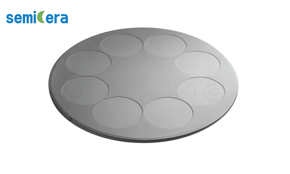
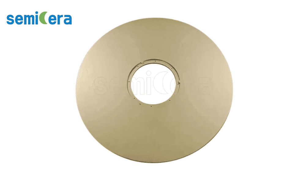
These coatings provide:
- Superior chemical resistance
- Higher temperature stability
- Improved surface durability
- Reduced contamination risk
For advanced epitaxy manufacturing, the quality of thermal management components directly affects production yield and wafer consistency.
2. gas flow control
Inside an MOCVD reactor, precursor gases must be distributed evenly across the wafer surface. Poor gas dynamics may result in:
- Edge effects
- Thickness variation
- Non-uniform composition
Therefore, reactor design, showerhead structure, and process optimization are critical factors in achieving high-quality epitaxial growth.
3. production cost
MOCVD requires expensive equipment, high-purity materials, and sophisticated process control systems. Manufacturers must balance:
- Film quality
- Production efficiency
- Equipment cost
- Long-term reliability
Making the Right Choice for Your Goal
Selecting the right MOCVD technology depends heavily on the target application.
- For LED manufacturing, high throughput and excellent thickness uniformity are major priorities.
- For GaN power devices, crystal quality and defect control become more important.
- For advanced research applications, flexible process control and material compatibility are often the key requirements.
Ⅵ. Ready to Integrate Advanced MOCVD Technology into Your Lab?
As semiconductor manufacturing continues moving toward larger wafers, higher power density, and more demanding applications, MOCVD technology will remain a critical platform for next-generation device fabrication.
Whether your goal is developing advanced GaN devices, improving LED efficiency, or exploring future compound semiconductor technologies, selecting reliable MOCVD components and thermal management solutions is essential.
Advanced materials such as CVD SiC coated graphite components, TaC coated susceptors, and high-performance semiconductor thermal solutions are helping manufacturers achieve higher process stability, better uniformity, and improved production efficiency.
The future of semiconductor innovation begins with precise control at the atomic level — and MOCVD remains one of the most powerful technologies making that possible.
Post time: Jul-31-2026