
SiC Wafer Bonding: Methods, Uses and Challenges
Two wafers can look perfectly flat and still refuse to bond reliably. At the scale that matters, surface chemistry, atomic roughness, particles and trapped gases decide whether contact becomes a durable interface. Silicon carbide raises the difficulty further: it is chemically stable, mechanically hard and often paired with materials that expand or conduct heat very differently.
Why bond SiC wafers at all?
Silicon carbide is valued because it combines a wide bandgap with high breakdown strength, thermal conductivity and chemical stability. Those same properties make SiC difficult to process, integrate and thermally manage. Wafer bonding addresses that tension by separating functions: one layer can provide the active crystal or device surface, while another supplies electrical conduction, heat spreading, mechanical support or optical access.
This is why wafer bonding is more than a joining step. The interface becomes part of the device architecture. Its thickness, chemistry, defects, stress and thermal boundary resistance can determine whether a promising material stack works at wafer scale. Semicera’s technical department and researchers have also conducted in-depth studies on this to pursue the best balance and outcome.
Direct versus indirect bonding
Direct bonding joins two prepared surfaces without a conventional adhesive or thick solder layer. The attraction may begin with van der Waals forces, hydrogen bonding, electrostatic forces or newly created surface bonds, followed by pressure or annealing. Indirect bonding inserts a metal, eutectic, polymer, solder or nanoscale adhesive layer. The intermediate layer can simplify joining, but it may add thermal resistance, electrical loss, contamination or high-temperature reliability concerns.
For SiC, direct methods are attractive when the application demands a thin, clean and thermally efficient interface. Indirect methods remain useful when surface flatness, process temperature, material compatibility or production cost makes direct bonding impractical. The correct comparison is therefore application-specific rather than ideological.
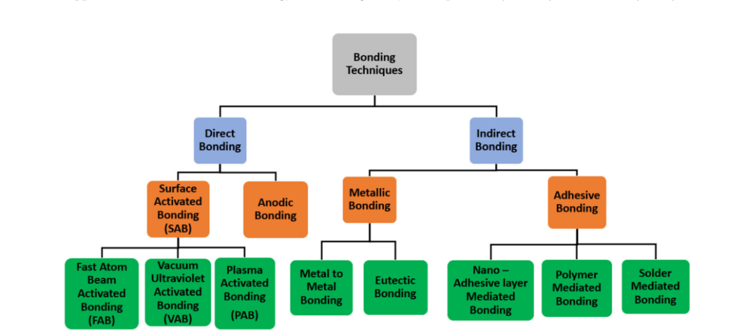
Surface activation routes
Fast-atom-beam surface-activated bonding removes native oxides and contaminants in ultra-high vacuum and exposes reactive surface sites. Bonding can occur near room temperature, but ion or atom bombardment may create an amorphous or damaged surface layer if activation is too aggressive.
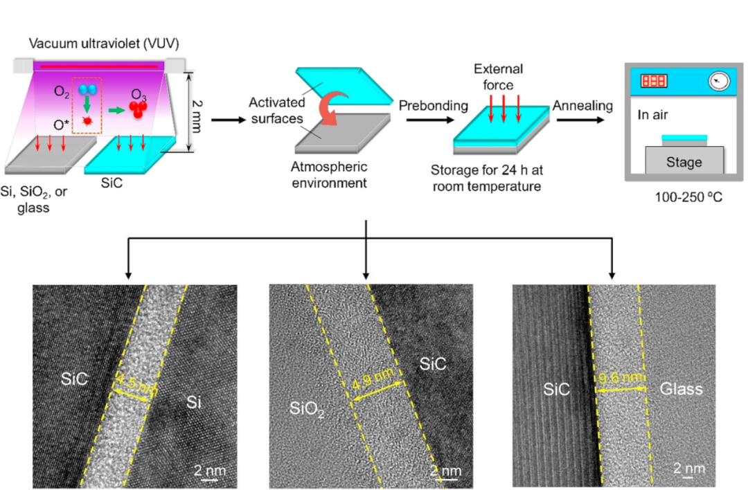
Vacuum-ultraviolet activation uses short-wavelength radiation to generate reactive oxygen species and surface groups. It can support low-temperature bonding with less particle loading than some plasma tools, although the result depends strongly on initial surface chemistry and exposure conditions.
Plasma-activated bonding modifies surface energy and often makes the surface hydrophilic. Pre-bonding can then occur in ambient conditions, followed by a moderate-temperature anneal. Atmospheric plasma approaches are particularly interesting for throughput, but uniform activation and contamination control must be maintained over the full wafer.
Anodic bonding uses heat and a strong electric field to move mobile ions in glass and build an electrostatic attraction at the interface. It is established for selected semiconductor-to-glass combinations, but its material set and thermal budget are narrower than general-purpose direct bonding.
Four application directions
- Engineered SiC substrates: Soitec’s SmartSiC™ platform uses Smart Cut™ technology to transfer a thin, high-quality mono-SiC layer onto a low-resistivity poly-SiC handle substrate. The architecture separates the epi-ready active surface from the conductive support and enables donor-wafer reuse.
- Power packaging and heat extraction: A 2025 study reported direct SiC/Cu bonding with approximately 57 MPa bonding strength and thermal boundary conductance of about 0.128 GW·m⁻²·K⁻¹. The result illustrates why oxide-free, solder-free interfaces are being explored for high-temperature power systems.
- III–V/SiC heterogeneous integration: A 2024 study used hydrophilic direct bonding for InP/SiC at room temperature and reported an average bonding strength of 3.2 MPa and thermal conductivity of 112.60 W·m⁻¹·K⁻¹. The concept pairs InP’s optoelectronic function with SiC heat spreading.
- Composite wafer platforms: commercial development is moving toward a functional upper layer joined to a support substrate chosen for thermal, mechanical or electrical performance. These stacks can reduce the need to ask one crystal to provide every function simultaneously.
The metrics that matter
Semicera noticed that bond strength is necessary, but it is not sufficient. A useful qualification plan also measures void density, interfacial layer thickness, chemical residues, crystal damage, bow and warp, thermal boundary conductance, electrical contact resistance and reliability after thermal cycling. Optical and acoustic applications add absorption, scattering and acoustic impedance requirements.
For Semicera, wafer-scale uniformity is the manufacturing gate. A small-area interface can look excellent in microscopy while a production wafer still fails because surface roughness, particles, activation dose, pressure or temperature varies across the diameter. Metrology must therefore connect atomic-scale analysis with in-line inspection and statistical process control.
Why SiC bonding remains difficult?
SiC surfaces are chemically stable and relatively hard to activate. Strong treatments can improve reactivity but damage the lattice or leave an amorphous layer. Heterogeneous pairs add mismatch in thermal expansion, elastic modulus, lattice structure and surface chemistry, so stress may accumulate during annealing or service.
The best process window is a balance: enough activation to form a continuous bond, but low enough damage and temperature to preserve the device layer. That balance changes with wafer diameter, doping, crystal face, polish, partner material and end-use environment. Meanwhile, Semicera always keep it.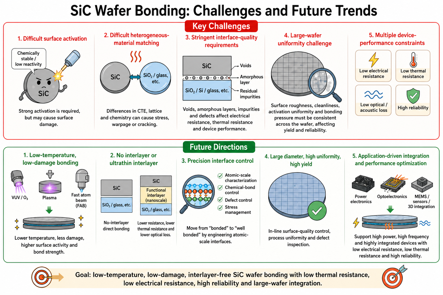
Technology roadmap
The direction is toward lower-temperature, lower-damage processes; no intermediate layer or an atomically thin functional interface; precise control of interface chemistry; wafer-scale defect inspection; and co-optimization of bonding with the final device and package. Atmospheric activation and high-throughput metrology may become as important as record bond strength.
For Semicera’s engineers and buyers, the practical lesson is simple: specify the interface as a functional material system. Define the target electrical, thermal, optical and reliability performance first, then choose the activation, surface finish, anneal and inspection plan that supports those targets.
Engineering checklist
- · Define the required thermal, electrical, optical and mechanical interface functions.
- · Specify material pair, crystal face, diameter, thickness, doping and surface finish.
- · Set limits for particles, roughness, bow, warp, voids and edge exclusion.
- · Choose activation and annealing conditions within the device thermal budget.
- · Qualify both local interface quality and full-wafer uniformity.
- · Validate reliability through thermal cycling, aging and application-relevant stress.
Conclusion
SiC wafer bonding is becoming a practical route to engineered substrates, high-temperature packaging and heterogeneous integration. Its value comes from assigning different functions to different materials. Its difficulty comes from the interface: activation, contamination, stress and wafer-scale uniformity must all be controlled at once. The most credible development programs therefore treat bonding, metrology and end-use performance as one integrated problem.
Semicera perspective: When bonded-wafer development depends on high-purity SiC, graphite, coated process components or thermal-management materials, early alignment between material specifications and process conditions can reduce qualification cycles.
Post time: Sep-02-2026