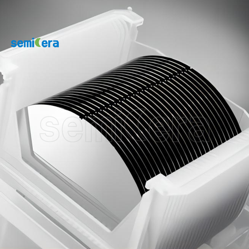
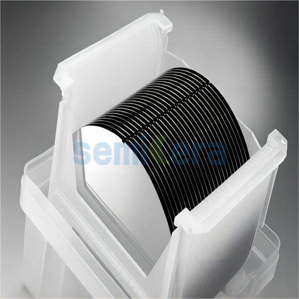
GaAs substrates are divided into conductive and semi-insulating, which are widely used in laser (LD), semiconductor light-emitting diode (LED), near-infrared laser, quantum well high-power laser and high-efficiency solar panels. HEMT and HBT chips for radar, microwave, millimeter wave or ultra-high speed computers and optical communications; Radio frequency devices for wireless communication, 4G, 5G, satellite communication, WLAN.
Recently, gallium arsenide substrates have also made great progress in mini-LED, Micro-LED, and red LED, and are widely used in AR/VR wearable devices.
|
Diameter |
50mm | 75mm | 100mm | 150mm |
|
Growth Method |
LEC 液封直拉法 |
|
Wafer Thickness |
350 um ~ 625 um |
|
Orientation |
<100> / <111> / <110> or others |
|
Conductive Type |
P – type / N – type / Semi-insulating |
|
Type/Dopant |
Zn / Si / undoped |
|
Carrier Concentration |
1E17 ~ 5E19 cm-3 |
|
Resistivity at RT |
≥1E7 for SI |
|
Mobility |
≥4000 |
|
EPD( Etch Pit Density ) |
100~1E5 |
|
TTV |
≤ 10 um |
|
Bow / Warp |
≤ 20 um |
|
Surface Finish |
DSP/SSP |
|
Laser Mark |
|
|
Grade |
Epi polished grade / mechanical grade |