Silicon carbide (SiC) single crystal material has a large band gap width (~Si 3 times), high thermal conductivity (~Si 3.3 times or GaAs 10 times), high electron saturation migration rate (~Si 2.5 times), high breakdown electric field (~Si 10 times or GaAs 5 times) and other outstanding characteristics.
SiC devices have irreplaceable advantages in the field of high temperature, high pressure, high frequency, high power electronic devices and extreme environmental applications such as aerospace, military, nuclear energy, etc., make up for the defects of traditional semiconductor material devices in practical applications, and are gradually becoming the mainstream of power semiconductors.
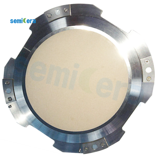
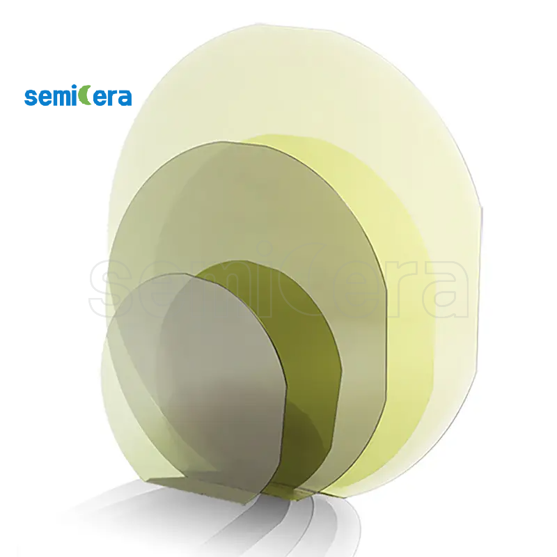
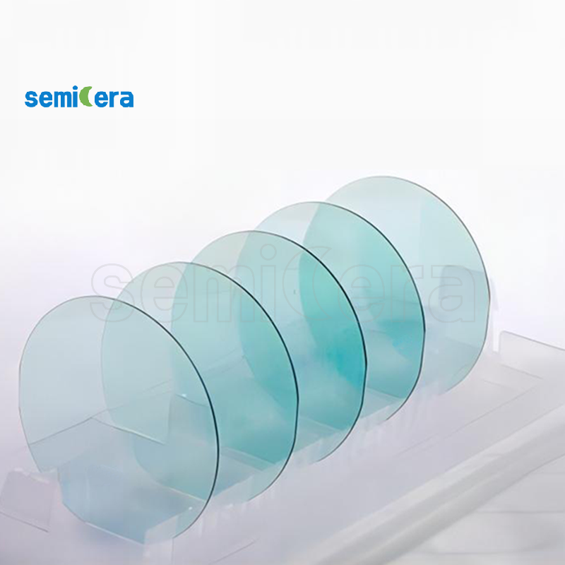
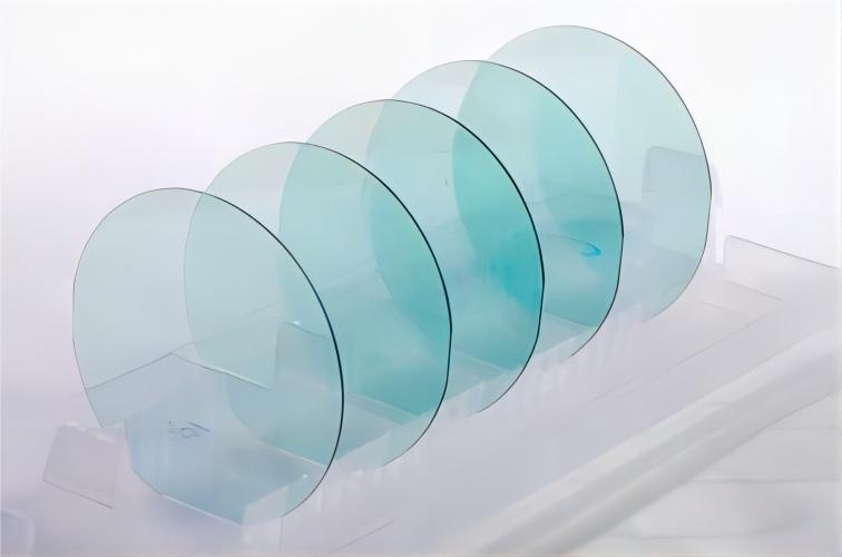
4H-SiC Silicon carbide substrate specifications
|
Item项目 |
Specifications参数 |
|
|
Polytype |
4H -SiC |
6H- SiC |
|
Diameter |
2 inch | 3 inch | 4 inch | 6inch |
2 inch | 3 inch | 4 inch | 6inch |
|
Thickness |
330 μm ~ 350 μm |
330 μm ~ 350 μm |
|
Conductivity |
N – type / Semi-insulating |
N – type / Semi-insulating |
|
Dopant |
N2 ( Nitrogen )V ( Vanadium ) |
N2 ( Nitrogen ) V ( Vanadium ) |
|
Orientation |
On axis <0001> |
On axis <0001> |
|
Resistivity |
0.015 ~ 0.03 ohm-cm |
0.02 ~ 0.1 ohm-cm |
|
Micropipe Density(MPD) |
≤10/cm2 ~ ≤1/cm2 |
≤10/cm2 ~ ≤1/cm2 |
|
TTV |
≤ 15 μm |
≤ 15 μm |
|
Bow / Warp |
≤25 μm |
≤25 μm |
|
Surface |
DSP/SSP |
DSP/SSP |
|
Grade |
Production / Research grade |
Production / Research grade |
|
Crystal Stacking Sequence |
ABCB |
ABCABC |
|
Lattice parameter |
a=3.076A , c=10.053A |
a=3.073A , c=15.117A |
|
Eg/eV(Band-gap) |
3.27 eV |
3.02 eV |
|
ε(Dielectric Constant) |
9.6 |
9.66 |
|
Refraction Index |
n0 =2.719 ne =2.777 |
n0 =2.707 , ne =2.755 |
6H-SiC Silicon Carbide substrate specifications
|
Item项目 |
Specifications参数 |
|
Polytype |
6H-SiC |
|
Diameter |
4 inch | 6inch |
|
Thickness |
350μm ~ 450μm |
|
Conductivity |
N – type / Semi-insulating |
|
Dopant |
N2( Nitrogen ) |
|
Orientation |
<0001> off 4°± 0.5° |
|
Resistivity |
0.02 ~ 0.1 ohm-cm |
|
Micropipe Density(MPD) |
≤ 10/cm2 |
|
TTV |
≤ 15 μm |
|
Bow / Warp |
≤25 μm |
|
Surface |
Si Face: CMP, Epi-Ready |
|
Grade |
Research grade |