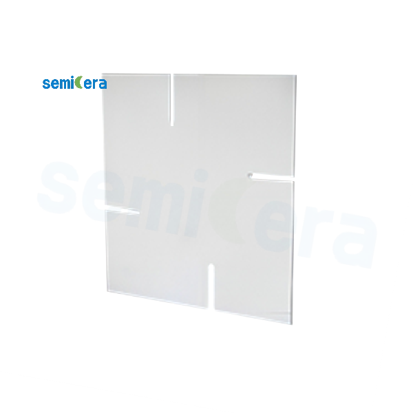
Materials and Properties of Quartz Semiconductor Etch Rings
Semicera quartz etching rings are manufactured from semiconductor-grade fused quartz (SiO₂), selected for its exceptional purity, dielectric stability, and compatibility with aggressive plasma processing environments.
Fused quartz possesses an amorphous microstructure with extremely low metallic impurity levels, making it an ideal material for applications where contamination control is essential. Unlike metallic or conductive materials, quartz functions as a stable dielectric medium that influences local electric field distribution within the plasma chamber. This characteristic enables quartz etch rings to help regulate plasma boundary conditions and contribute to improved process uniformity across the wafer surface.
Key material advantages include:
● Ultra-high purity and low metallic contamination
● Excellent dielectric properties
● High resistance to thermal shock
● Low coefficient of thermal expansion
● Stable performance under vacuum conditions
● Excellent compatibility with fluorine-based and chlorine-based plasma chemistries
● Low particle generation when properly maintained
The combination of these properties allows quartz etch rings to maintain dimensional stability and process consistency during repeated thermal and plasma exposure cycles.
Applications
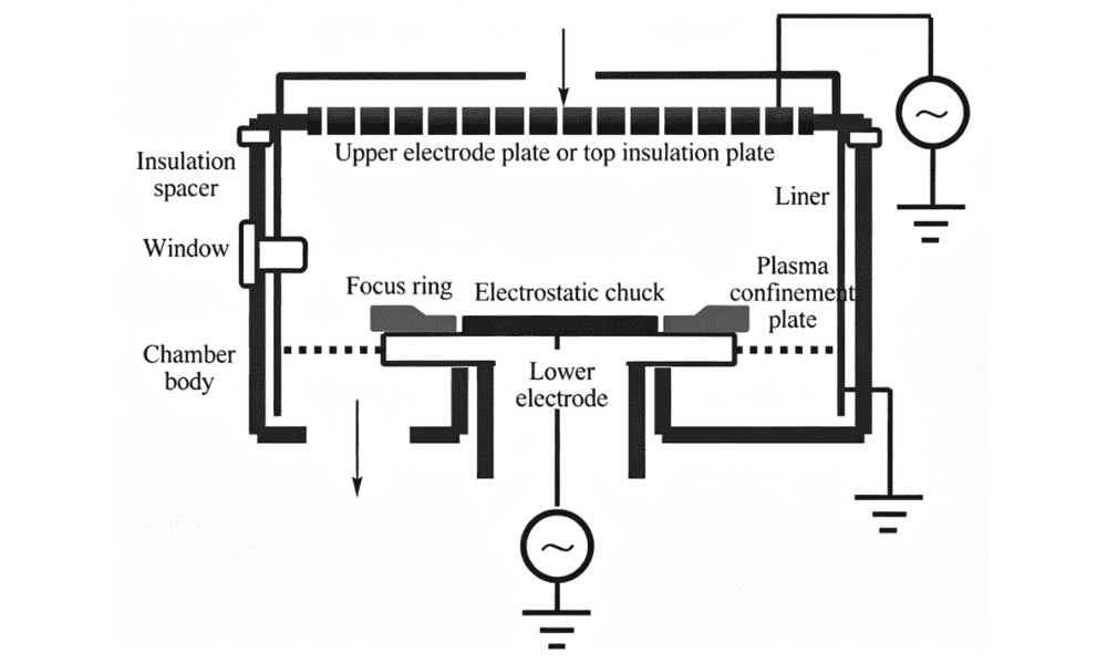
In modern plasma etching systems, quartz etch rings perform multiple functions that extend beyond mechanical support. Positioned around the wafer processing area, the ring serves as a critical interface between the plasma region and surrounding chamber structures. Through its dielectric characteristics, the quartz ring helps shape local electric field distributions, stabilize plasma sheath behavior, and reduce edge-related process variations.
Quartz semiconductor etching rings are widely utilized in advanced etch applications including silicon etching, dielectric etching, polysilicon processing, deep reactive ion etching (DRIE), MEMS fabrication, power semiconductor manufacturing, and compound semiconductor production. In high-density plasma environments, the ring contributes to improved wafer edge uniformity by minimizing plasma distortion and controlling ion flux distribution near the wafer perimeter.
In addition to plasma control functions, quartz etch rings also serve as protective chamber components that help reduce direct plasma exposure to critical hardware surfaces. By acting as a controlled consumable interface, they assist in maintaining chamber cleanliness, extending maintenance intervals, and supporting stable process performance throughout production cycles.
As advanced semiconductor manufacturing moves toward increasingly stringent requirements for critical dimension control and defect reduction, quartz etch rings remain an essential component in achieving repeatable and reliable plasma processing results.
Technical Data of Fused Quartz Materials
The following properties represent typical values for semiconductor-grade fused quartz materials used in Semicera etching ring manufacturing.
|
Property |
Typical Value |
|
Material Composition |
≥99.99% SiO₂ |
|
Density |
2.20 g/cm³ |
|
Softening Point |
Approx. 1730°C |
|
Annealing Point |
Approx. 1215°C |
|
Thermal Expansion Coefficient |
5.5 × 10⁻⁷ /°C |
|
Dielectric Constant (1 MHz) |
3.75 – 3.90 |
|
Electrical Resistivity |
>10¹⁸ Ω·cm |
|
Thermal Conductivity |
1.3 – 1.5 W/m·K |
|
Mohs Hardness |
5.5 – 6.5 |
|
Operating Environment |
Vacuum, Plasma, High-Purity Gas Systems |
Customization Advantages
Semicera provides comprehensive customization capabilities to meet the evolving requirements of semiconductor equipment manufacturers and process engineers.
Our engineering team works closely with customers to optimize component geometry, dimensional tolerances, and material specifications based on specific chamber designs and process conditions. Through precision CNC machining and advanced inspection technologies, we are able to manufacture quartz etch rings with complex profiles, tight tolerance control, and excellent surface quality.
Customization options include:
✔ Custom outer and inner diameters
✔ Complex plasma control geometries
✔ Multi-step and profiled ring structures
✔ Precision groove and slot machining
✔ Surface finish optimization
✔ Semiconductor-grade cleaning and packaging
✔ Prototype and volume production support
By combining high-purity fused quartz materials with advanced manufacturing expertise, Semicera delivers tailored quartz etch ring solutions designed to support process stability, contamination control, and long-term operational reliability in semiconductor plasma processing equipment.