Silicon wafer (Si Wafer)
What is a silicon wafer?
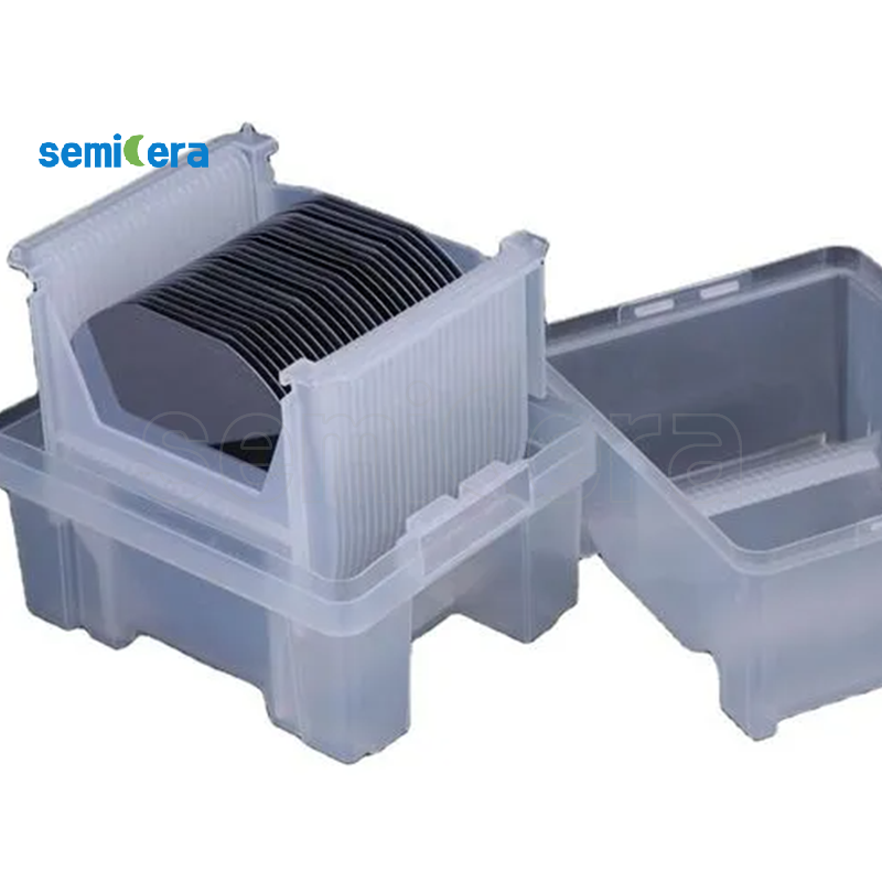
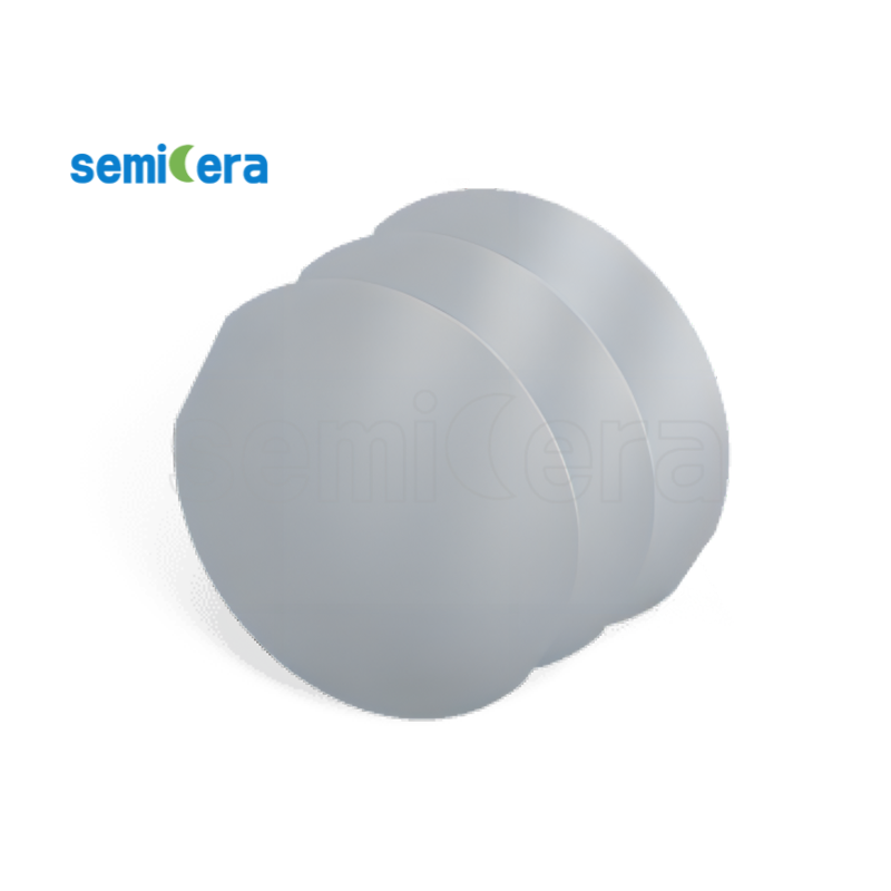
A silicon wafer is a circular thin sheet fabricated by cutting, grinding, and polishing high-purity monocrystalline silicon ingots; it serves as the fundamental substrate material for the manufacturing of integrated circuits, power devices, MEMS sensors, photovoltaic and optical components. The electrical properties of the wafer (resistivity, doping type), geometric accuracy (thickness, TTV, warpage), and surface quality (roughness, particle size) directly determine the yield and device consistency in subsequent processes such as epitaxial growth, photolithography, and coating; therefore, the selection and traceability of wafers are critical for customer production lines.
Semicera Laboratory's silicon wafer product portfolio spans a wide range of segments, from bare wafer substrates to functional substrates; it allows for the customization of various crystal growth techniques, cutting orientations, and surface treatment solutions based on downstream fabrication processes (epitaxy, oxidation, bonding, MEMS processing).
Product line
This category includes the following sub-products, each available in customized specifications:
|
Product |
Main features |
Typical Applications |
|
Ultra-thin silicon layer with thickness controllable down to the submicron range |
SOI device layer, thin-film sensor |
|
|
High surface flatness – single-or double-sided polishing |
MEMS and power devices; epitaxial growth; general process verification |
|
|
CZ method – wide resistivity range |
IC manufacturing, discrete devices |
|
|
District melting (without crucible), ultra-high resistivity, low oxygen content |
Power devices, detectors, high-frequency/RF applications |
|
|
Surface-grown SiO₂ insulating layer with controllable thickness |
MEMS isolation layer and capacitor/dielectric research |
Core Technical Specifications
The following lists common customizable specification ranges for silicon wafer products; the exact values are subject to the Order Confirmation Form:
|
Parameter |
Typical Range |
Explain |
|
Wafer diameter |
2″ – 12″ (50–300 mm) |
Supports custom small-sized sample sheets |
|
Crystal growth mode |
CZ (Czochralski method) / FZ (Zone melting method) |
FZ is designed for ultra-high resistivity and low-oxygen environments. |
|
crystal orientation |
(100)、(111)、(110) |
Matched to downstream process requirements |
|
Doping type |
N-type / P-type |
Doping elements: phosphorus, arsenic, boron, etc. |
|
resistivity |
0.001 – 10,000 Ω·cm |
The FZ process enables operation in the high-resistance region. |
|
thickness deviation |
±10–25 μm (depending on size) |
As the diameter increases, the standard thickness increases accordingly. |
|
Total Thickness Variation (TTV) |
≤ 1–5 μm |
Affects photolithography depth of field and bonding consistency |
|
Warp/Bow |
≤ 5–20 μm |
Large-format sheets require more stringent warpage control measures. |
|
Surface roughness (Ra) |
Sub-nanometer scale (polished surface) |
Affects thin-film adhesion and device electrical performance |
|
edge processing |
Circular edge/Chamfer – compliant with SEMI standards |
Reduce edge cracking and particle contamination |
|
surface state |
Single-sided polishing (SSP)/Double-sided polishing (DSP) |
DSP is suitable for bonding and MEMS fabrication processes. |
Note: The CZ method employs a quartz crucible for crystal growth; this process is well-established and cost-effective, but the oxygen introduced by the crucible limits the maximum resistivity value. In contrast, the FZ method does not use a crucible, resulting in an extremely low oxygen content and enabling the production of higher and more uniform resistivity values – making it particularly suitable for high-resistance applications such as power devices and detectors. This difference in manufacturing processes serves as a key criterion when selecting a material or fabrication method.
Production and Testing Process

The entire process is carried out within a controlled cleanroom environment; for all critical processes, detailed inspection data records are maintained to ensure consistent and traceable parameters across batches.
Application area
- • Integrated circuit manufacturing: As a substrate material for standard logic and memory devices
- • Power semiconductors: IGBTs, MOSFETs, Schottky diodes, and other devices sensitive to high resistance and low defect density.
- • MEMS and Sensors: Utilizing double-sided polished wafers and thermal oxidation wafers to fabricate structural and isolation layers.
- • RF/High-Frequency Devices: High-resistance silicon substrates reduce dielectric loss, making them suitable for 5G filters and switch modules.
- • Photovoltaics and Optics: As a substrate for coating and optical reference specimens
- • Research and Process Validation: Small-scale customized sample wafers for laboratory and pilot-scale production lines
Why choose us?
- Integrated materials capability: The company maintains comprehensive product lines encompassing silicon carbide (SiC) coatings, quartz, graphite, carbon fiber, and wafer products, enabling it to provide end-to-end material support to semiconductor equipment and wafer manufacturing customers – rather than merely offering standalone product supplies.
- Customized production: Non-standard customization is available based on specific process parameters provided by the customer (e.g., resistivity, crystal orientation, thickness, TTV), and small-batch sample validation is supported.
- Quality System and Testing Capabilities: The production process is subject to testing in accordance with SEMI standards (all-or-none or random sampling of key parameters such as resistivity, TTV, warpage, and surface particle size); relevant qualifications and certification information can be found on the Qualifications and Honors page.
Frequently Asked Questions (FAQ)
Q: How should one choose between CZ silicon wafers and FZ silicon wafers?
A: For applications where cost is a primary concern and the resistivity requirement falls within a low-to-medium range, CZ silicon wafers represent a more economical choice; however, for applications (e.g., high-voltage power devices or detectors) that demand extremely high and uniform resistivity along with an extremely low oxygen content, FZ silicon wafers are recommended.
Q: What is the difference between single-sided polishing (SSP) and double-sided polishing (DSP)?
A: SSP features a mirror-like surface finish on only one side and offers lower cost, making it suitable for conventional epitaxial and photolithography processes; DSP features polished surfaces on both sides, providing higher flatness and superior backside cleanliness, and is commonly used in bonding, MEMS applications, or processes where stringent backside quality requirements are imposed.
Q: Does the service support non-standard dimensions or small-batch prototyping?
A: Support – The diameter, thickness, crystallographic orientation, and surface treatment can be customized according to the customer’s drawings or specification requirements; sample specimens will be provided for verification before proceeding to mass production.
Q: How can we confirm whether the wafer parameters meet our production line requirements?
A: We recommend providing the target resistivity range, crystal orientation, thickness tolerance, TTV/deflection requirements, and surface condition (SSP/DSP); based on these specifications, we will provide selection recommendations and a testing report.
Request a Quote and Technical Documentation
To obtain quotes for specific silicon wafer specifications, download the product technical parameters sheet, or discuss customized non-standard solutions, please submit your request via the “Contact Us” , we will respond within 24 hours.