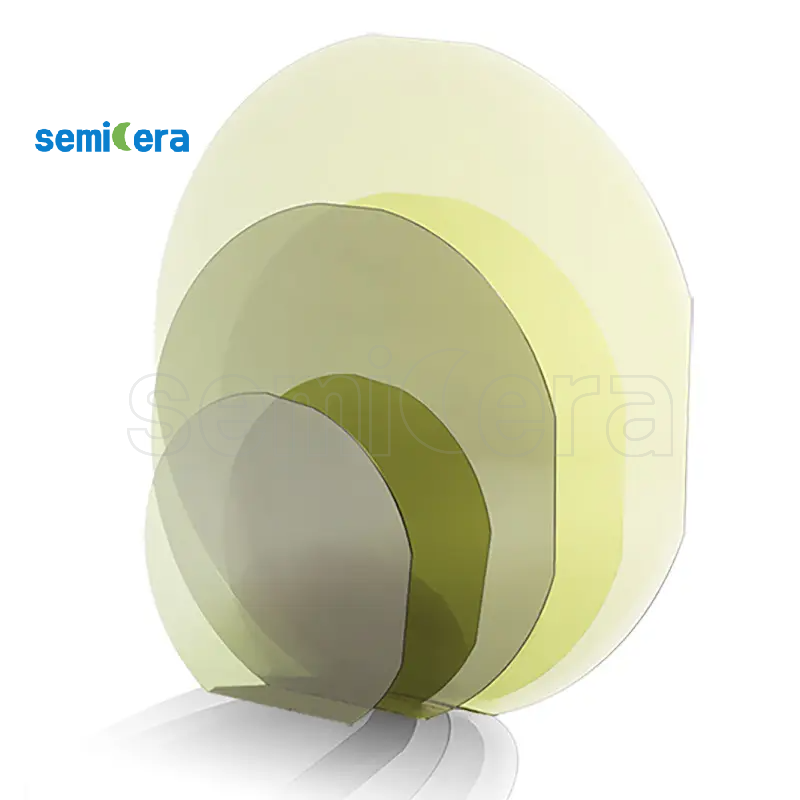
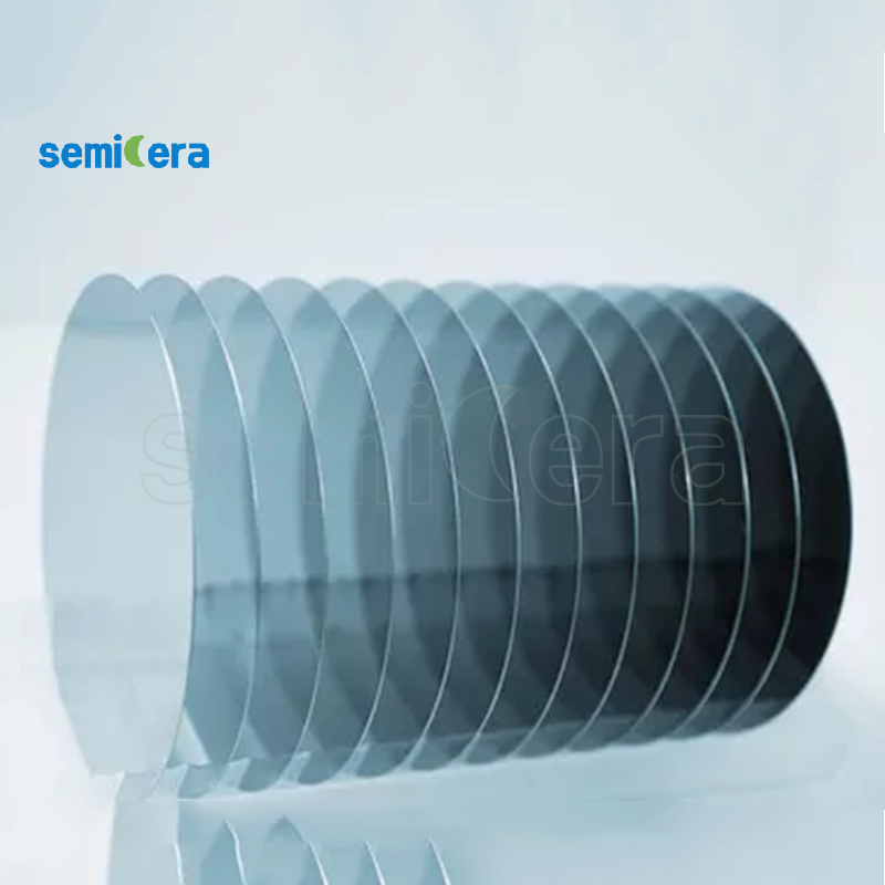
Epi-Wafer
Semicera supplies epitaxial wafers for compound and elemental semiconductor device fabrication, including GaN, silicon (Si), and silicon carbide (SiC) epitaxial wafers. Its product range spans standard N-type/P-type epitaxial layers to high-power GaN-on-Si structures, supporting diameters from research-scale samples up to 6-inch (150mm) production wafers.
Depending on the target device — power, RF, optoelectronic, or sensor applications — epitaxial wafers require precise control of epitaxial layer thickness, doping concentration, resistivity, and surface/defect quality. Semicera can support material selection, substrate and epitaxial-layer specification, and customization based on customer device requirements, target electrical parameters, or reference samples.
Product line
This category encompasses epitaxial wafers customized to meet the diverse requirements of various semiconductor device platforms and fabrication processes. (Insert URL for each product)
|
Product type |
Major function |
Typical Applications |
|
GaN epitaxial layer grown on a compatible substrate for high electron mobility structures |
RF devices, power electronics, LED/laser epitaxy |
|
|
Silicon epitaxial layer with controlled doping type and resistivity |
CMOS, power devices, sensor fabrication |
|
|
SiC epitaxial layer grown on SiC substrate for wide-bandgap device structures |
Power devices, high-voltage and high-temperature electronics |
|
|
GaN epitaxial structure on silicon substrate engineered for high-voltage power switching |
Power conversion, fast charging, motor drive systems |
|
|
Large-diameter N-type silicon epitaxial wafer for volume production |
Power semiconductor and integrated circuit manufacturing |
Core Technology Considerations
Epitaxial wafers are typically customized based on target device application, material system, and electrical specification. During technical consultations, the following parameters can be evaluated.
|
Parameter |
Customization Scope |
|
Substrate material |
Silicon, silicon carbide, sapphire, or other substrates selected according to device requirements |
|
Epitaxial layer material |
GaN, Si, SiC, or other compound/elemental semiconductor materials |
|
Doping type & concentration |
N-type or P-type, with customized doping concentration and resistivity range |
|
Wafer diameter |
2" / 4" / 6" (150mm), and other sizes available upon request |
|
Epitaxial layer thickness |
Controlled based on customer specification and target device design |
|
Surface & defect quality |
Customized inspection standards for surface roughness, defect density, and particle control |
|
Order quantity |
Prototype evaluation, sample production, and batch delivery |
Note: The final technical specifications shall be confirmed in accordance with the customer's target parameters, device design, reference sample, and actual process requirements.
Typical Applications
- Power electronics: High-voltage, high-power GaN-on-Si and SiC epitaxial wafers for power switching and conversion devices.
- RF and high-frequency devices: GaN epitaxial structures supporting high electron mobility transistor (HEMT) fabrication.
- Optoelectronic devices: Epitaxial wafers supporting LED, laser diode, and photodetector fabrication.
- Integrated circuit and sensor manufacturing: Silicon epitaxial wafers with controlled doping for CMOS and sensor applications.
- Semiconductor device manufacturers: Custom epitaxial wafers developed according to target electrical parameters, technical specifications, or reference samples.
Customized manufacturing processes
Semicera supports a structured custom development process for epitaxial wafers:
1. Customer specification / target parameters / Reference sample
2. Material and Process Assessment
3. Substrate Selection and Verification
4. Epitaxial Growth Trial
5. Layer Thickness and Doping Control
6. Surface Inspection and Defect Control
7. Electrical and Structural Testing
8. Sample Approval
9. Mass Production
Why choose Semicera?
- Integrated Material Capability: Semicera's material and product portfolio encompasses epitaxial wafers, silicon carbide coatings, graphite components, silicon carbide ceramic products, quartz materials, and carbon fiber materials. This portfolio supports cross-material evaluation across power, RF, and optoelectronic device applications.
- Original OEM manufacturing and custom production: Customized epitaxial wafers can be assessed based on target electrical parameters, reference samples, or specified critical specifications provided by the customer; for non-standard material systems or structures, a feasibility review may be conducted prior to commencing production.
- From prototype to mass production support: This development process can support sample fabrication and technical validation prior to subsequent batch production; however, it is contingent upon material feasibility and confirmed specification parameters.
Frequently Asked Questions
Q: Can epitaxial wafers be customized according to my target electrical parameters?
Yes. Semicera can evaluate target resistivity, doping concentration, epitaxial layer thickness, and substrate specifications. Before production, it is essential to confirm material selection and process feasibility.
Q: Can Semicera match an existing epi-wafer sample?
A: For applicable scenarios, samples can be measured and evaluated for process matching; final feasibility depends on the material system, layer structure, and required tolerances.
Q: What wafer sizes are available?
A: Standard sizes range from 2-inch to 6-inch (150mm), with other diameters available upon request depending on material system and equipment capability.
Q: What information do I need to provide to get a quote?
A: We recommend providing substrate material, epitaxial layer material, doping type and concentration, layer thickness, wafer diameter, and estimated quantity.
Request for Quotation and Technical Assessment
To obtain a quotation for epitaxial wafers, please provide your target specifications, reference sample information, or device requirements. Semicera can assess material feasibility, layer design, and production timeline before proceeding with sample development or mass production.
Please contact Semicera to discuss your specific requirements for custom epitaxial wafers.