1.About Silicon Carbide (SiC) Epitaxial Wafers
Silicon Carbide (SiC) epitaxial wafers are formed by depositing a single crystal layer on a wafer using a silicon carbide single crystal wafer as a substrate, usually by chemical vapor deposition (CVD). Among them, silicon carbide epitaxial is prepared by growing silicon carbide epitaxial layer on the conductive silicon carbide substrate, and further fabricated into high-performance devices.
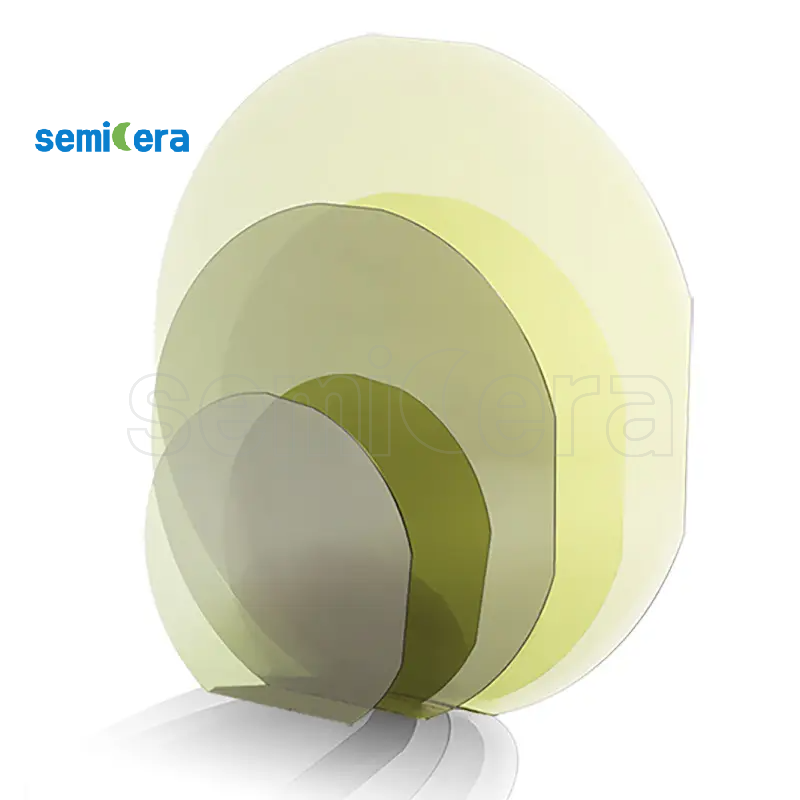
2.Silicon Carbide Epitaxial Wafer Specifications
We can provide 4, 6, 8 inches N-type 4H-SiC epitaxial wafers. The epitaxial wafer has large bandwidth, high saturation electron drift speed, high speed two-dimensional electron gas, and high breakdown field strength. These properties make the device high temperature resistance, high voltage resistance, fast switching speed, low on-resistance, small size and light weight.
3. SiC Epitaxial Applications
SiC epitaxial wafer is mainly used in Schottky diode (SBD), metal oxide semiconductor field effect transistor (MOSFET) junction field effect transistor (JFET), bipolar junction transistor (BJT), thyristor (SCR), insulated gate bipolar transistor (IGBT), which is used in low-voltage, medium-voltage and high-voltage fields. Currently, SiC epitaxial wafers for high-voltage applications are in the research and development stage worldwide.