Product overview
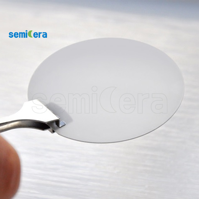
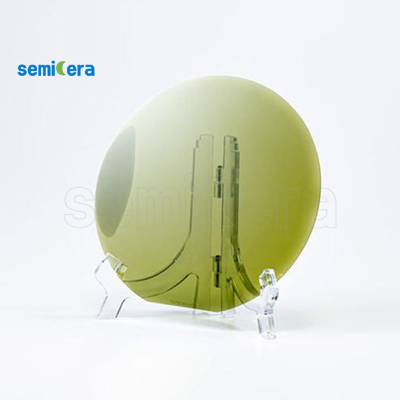
A semi-insulating SiC wafer platform combining high resistivity with SiC’s thermal and mechanical advantages. Available in 4H or 6H polytype and diameters from 2 to 12 inches for optical-window, heat-spreading and heterogeneous-integration evaluation.
Key features
- · 2–12 inch diameter range
- · 4H or 6H polytype
- · Selected Z and test D grade options
- · High-resistivity specification
- · Double-side polish with controlled flatness and defect criteria
Typical applications
- · Optical windows and harsh-environment optics
- · Heat spreaders for high-power devices
- · RF and microwave substrate evaluation
- · Heterogeneous integration and bonded wafer research
- · Transparent protective and sensing platforms
Technical specification
|
Property |
Selected Z |
Test D |
|
Diameter |
2–12 in |
2–12 in |
|
Polytype |
4H / 6H |
4H / 6H |
|
Thickness |
350–500 µm ±15 µm / bulk |
350–500 µm ±15 µm / bulk |
|
Off-axis from <0001> |
<0.5° |
<0.5° |
|
Micropipe density |
≤0.5 cm⁻² |
≤5 cm⁻² |
|
Resistivity |
>1E10 Ω·cm |
>1E5 Ω·cm |
|
Primary flat / type |
(10-10) ±5° / notch |
(10-10) ±5° / notch |
|
Edge exclusion |
3 mm |
3 mm |
|
LTV / TTV |
≤2.5 / ≤6 µm |
≤5 / ≤15 µm |
|
Bow / warp |
≤25 / ≤40 µm |
≤40 / ≤60 µm |
|
Polished surfaces |
Both sides, Ra <1 nm |
Both sides, Ra <1 nm |
|
CMP roughness |
Ra 0.2 nm |
Ra ≤0.5 nm |
|
Hexagonal void cumulative area |
≤0.05% |
≤0.1% |
|
Polytype inclusions |
None |
Cumulative area ≤3% |
|
Visible inclusions |
≤0.05% |
≤3% |
|
Specification note: Values are reproduced from the supplied product specification. Final acceptance criteria, test methods and sampling plan must be confirmed in the quotation or purchase specification. |
||
Grade and order selection
1. State the intended application and process temperature or environment.
2. Specify grade, dimensions, orientation or polytype, thickness and surface finish.
3. Define the inspection method, defect limits and required certificate data.
4. Confirm sample quantity, annual demand, packaging and delivery expectations.
Frequently asked questions
Is the wafer fully transparent at every wavelength?
Optical transmission depends on wavelength, thickness, polytype, defects and surface finish. Please state the required spectral range and transmission target.
Which diameters are available?
The supplied range is 2 to 12 inches; feasibility should be confirmed for the exact polytype, thickness and grade.
What is the main grade difference?
Z grade carries tighter micropipe, flatness, resistivity and inclusion criteria than D grade.